Rethinking Superjunction’s Charge-Compensation Architecture with SuperQ
Why It Matters
SuperQ restores silicon’s cost‑performance edge in power electronics, offering a scalable alternative to expensive GaN solutions while enhancing reliability and efficiency.
Key Takeaways
- •High‑k dielectric replaces bulk p‑pillars, boosting conduction area
- •Asymmetric design cuts on‑resistance without sacrificing voltage rating
- •CMOS‑compatible ALD process enables low‑cost, high‑volume production
- •Silicon MOSFETs with SuperQ rival GaN on system‑level metrics
Pulse Analysis
The silicon limit—where specific on‑resistance scales with the 2.5 power of blocking voltage—has constrained power MOSFET efficiency for decades. Traditional superjunction (SJ) devices mitigated this by alternating n‑ and p‑type pillars, achieving multi‑dimensional depletion but sacrificing half the device area to blocking structures. As device dimensions shrink, further narrowing of pillar pitch becomes prohibitively complex, driving the industry to seek a new charge‑compensation method that preserves performance without inflating manufacturing cost.
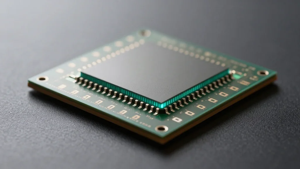
SuperQ’s breakthrough replaces the bulk p‑type pillars with a nanometer‑thin high‑k dielectric layer, such as alumina or hafnia, deposited by atomic‑layer deposition (ALD). This dielectric can sustain the required electric field while occupying as little as 5% of the device cross‑section, effectively reclaiming 95% of the silicon for current flow. The resulting asymmetric architecture delivers a more uniform electric field, markedly lower on‑resistance, and maintains high blocking voltages across a broad voltage spectrum (60 V‑1,200 V). Crucially, the process builds on mature CMOS and memory‑fab tools, allowing iDEAL to scale production without the steep capital outlay associated with wide‑bandgap (WBG) technologies.
From a market perspective, SuperQ re‑energizes silicon’s role in power conversion, offering a compelling cost‑performance balance against GaN and SiC devices. While GaN excels in switching loss, silicon MOSFETs with SuperQ provide superior avalanche capability, dV/dt immunity, and high‑temperature reliability—attributes vital for robust system design. By delivering mass‑produced, high‑voltage MOSFETs that combine efficiency with durability, iDEAL positions itself to capture applications where total cost of ownership and reliability outweigh pure performance metrics, potentially reshaping the power electronics supply chain.
Rethinking Superjunction’s Charge-Compensation Architecture with SuperQ
Comments
Want to join the conversation?
Loading comments...