Scaling the Next Generation of Multi-Die Systems
Companies Mentioned
Why It Matters
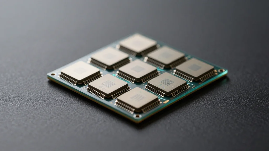
Scalable chiplet architectures are essential for meeting AI‑driven performance demands while controlling cost, making the transition from prototype to mass production a critical industry inflection point.
Key Takeaways
- •Chiplet adoption now focuses on production scalability challenges
- •EDA toolflows struggle with multi-die complexity and early design integration
- •Advanced packaging and interconnect standards like UCIe are critical for scaling
- •Industry leaders highlight bandwidth limits and need for silicon photonics
- •EE Times event provides roadmap for overcoming yield and thermal hurdles
Pulse Analysis
Chiplet technology has moved beyond proof‑of‑concept, becoming a cornerstone for AI‑centric processors that require massive compute density. By partitioning a system‑on‑chip into smaller, reusable dies, designers can accelerate time‑to‑market and mitigate lithography limits. However, the real test lies in scaling these heterogeneous blocks from lab benches to high‑volume fabs, where interconnect bandwidth, power delivery and thermal management become decisive factors. The EE Times conference gathers the ecosystem—foundries, EDA vendors, and system architects—to address these production‑grade hurdles.
A major bottleneck is the existing EDA toolchain, which was built for monolithic designs. As multi‑die architectures grow, physical design decisions must shift earlier in the flow, demanding AI‑enhanced simulation and physics‑informed models to predict signal integrity and thermal hotspots. Standards such as UCIe are evolving to provide a common language for inter‑die communication, yet the proliferation of interconnect types threatens to fragment the market. Advanced packaging techniques, including 2.5D/3D integration and co‑packaged optics, are being explored to push bandwidth beyond the limits of traditional copper traces.
Looking ahead, the convergence of silicon photonics, high‑density interposers and AI‑driven design automation promises to unlock the next wave of chiplet scalability. Industry leaders at the event stress that collaborative roadmaps—spanning design, manufacturing and testing—are essential to achieve reliable yields and manageable thermal density. As AI workloads continue to dominate data‑center and edge deployments, firms that master chiplet integration will secure a competitive edge, delivering higher performance per watt while reducing development cycles.
Scaling the Next Generation of Multi-Die Systems
Comments
Want to join the conversation?
Loading comments...