Semiconductors Enter 'Multi-Tasking' Era: New Device Cuts Required Components by 75% and Quadruples Processing Speed
Why It Matters
By consolidating several functions into one transistor, chip designers can dramatically shrink device footprints while delivering faster AI processing, a critical advantage for wearables and 3‑D integrated systems. The low‑temperature fabrication also eases integration into existing manufacturing lines, accelerating commercial adoption.
Key Takeaways
- •ZnO–Te heterojunction transistor reduces required transistors by 75%
- •Device achieves double negative differential transconductance for dual functions
- •Processing speed quadruples within a single signal cycle
- •Fabrication possible below 200 °C, compatible with back‑end‑of‑line limits
- •Enables ultra‑compact AI wearables and 3D integrated chips
Pulse Analysis
The semiconductor industry faces a paradox: devices are getting smaller while the computational load, especially from AI workloads, is exploding. Traditional scaling—adding more transistors to handle extra functions—runs into physical limits and rising costs. Engineers have responded by exploring heterogeneous integration and novel materials, but most solutions still require multiple components and complex interconnects. POSTECH’s ZnO‑Te heterojunction transistor breaks this pattern by embedding several circuit operations within a single crystal, offering a pathway to truly multi‑tasking chips that keep pace with the demand for edge AI.
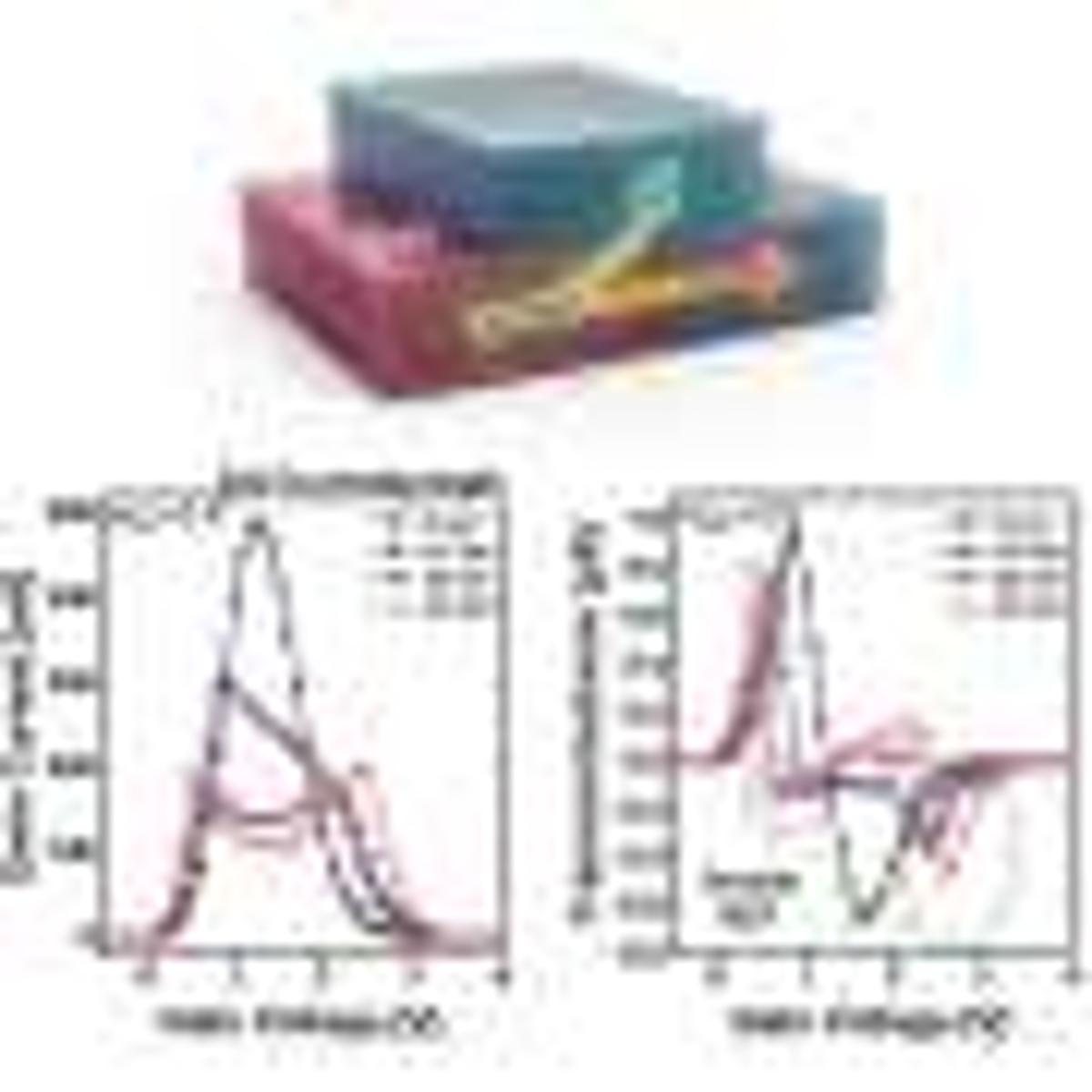
At the heart of the innovation is double negative differential transconductance (D‑NDT), a rare electrical behavior where current peaks twice as voltage varies. By adjusting the geometric overlap between ZnO and Te layers, the researchers coaxed lateral and vertical currents to coexist, producing two distinct current peaks in one device. This dual‑peak response enables functions such as frequency quadrupling without the need for separate transistors. Crucially, the materials can be deposited at temperatures under 200 °C, satisfying the sub‑400 °C ceiling imposed by back‑end‑of‑line processing and allowing seamless integration onto already‑fabricated chips.
The commercial implications are significant. A single transistor that replaces three or four conventional ones can slash bill of materials, reduce power consumption, and free up silicon real estate for additional features or smaller form factors. Wearable AI devices, which must balance performance with size and battery life, stand to benefit immediately. Moreover, the low‑temperature process aligns with existing foundry workflows, lowering barriers to volume production. As the industry moves toward three‑dimensional integrated circuits and heterogeneous stacking, technologies like POSTECH’s ZnO‑Te device could become foundational blocks for the next generation of ultra‑dense, high‑speed semiconductor systems.
Semiconductors enter 'multi-tasking' era: New device cuts required components by 75% and quadruples processing speed
Comments
Want to join the conversation?
Loading comments...