SiC Substrates with Table-Top Closed-Space PVT
Why It Matters
By cutting defect‑inducing thermal gradients and reducing operating temperature, CS‑PVT can lower production costs and improve yield for high‑voltage SiC power devices, accelerating market adoption of next‑generation electronics.
Key Takeaways
- •CS‑PVT reduces radial thermal gradients by an order of magnitude.
- •TableTopCS achieves 1900 °C growth temperature, saving energy.
- •Growth rates up to 300 µm/h enable thick 4H‑SiC layers.
- •Lower temperature cuts graphite hot‑zone wear, extending tool life.
- •Faster heat‑up/cool‑down shortens substrate production cycle.
Pulse Analysis
The rapid expansion of SiC wafer diameters—from 50 mm to emerging 300 mm formats—has outpaced the ability of traditional physical vapour transport (PVT) to maintain crystal quality. Standard PVT reactors generate steep radial thermal gradients at the 2000 °C crystallisation front, fostering dislocations that degrade power‑device reliability. As manufacturers push for larger, thinner boules to meet the demand for high‑voltage converters, the industry has sought a growth method that can tame these gradients without sacrificing throughput.
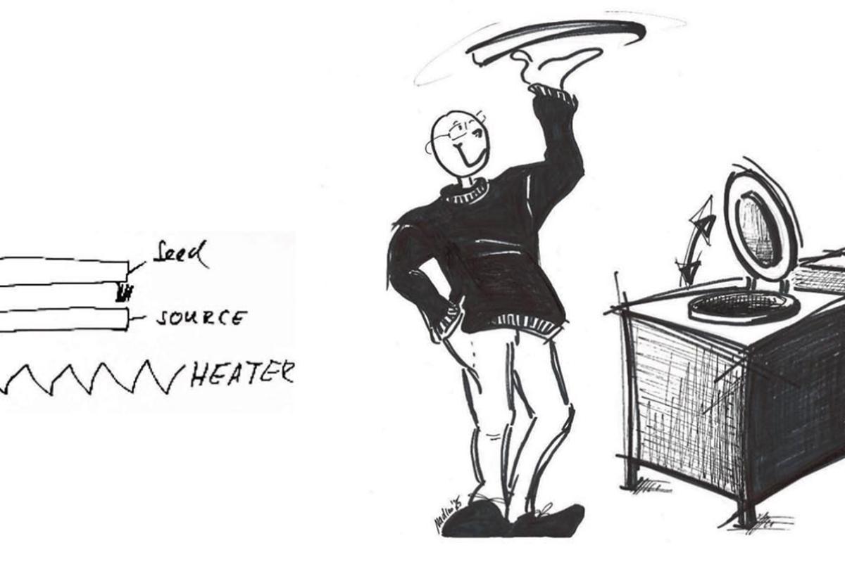
Close‑space PVT (CS‑PVT) addresses the core thermal challenge by confining the source‑to‑seed gap to roughly one millimetre and operating under ultra‑high vacuum. This geometry decouples the axial temperature gradient—driving crystal growth—from the radial gradient, allowing the furnace to run at about 1900 °C while preserving or even enhancing growth rates. The resulting ballistic mass‑transport regime improves dopant incorporation, especially for volatile acceptors like aluminium, and enables the deposition of thick, high‑purity 4H‑SiC layers at 300 µm per hour. The newly demonstrated tabletop CS‑PVT system combines a bottom‑heater for efficient heating with vacuum levels down to 10⁻⁸ mbar, making it adaptable to clean‑room environments, pilot lines, or academic labs.
From a commercial perspective, CS‑PVT offers several cost levers. Faster heating and cooling reduce cycle time, while the lower operating temperature cuts energy use and prolongs graphite hot‑zone life. Although individual boules may be shorter than those from conventional PVT, the ability to stack crucibles and the higher throughput can offset material usage. Moreover, CS‑PVT’s capability to grow intrinsic drift layers beyond the 50 µm ceiling of chemical vapour deposition opens pathways for 3‑kV‑plus SiC devices and novel photonic components. As the power‑electronics market seeks cheaper, defect‑free substrates, CS‑PVT stands poised to become a cornerstone of next‑generation SiC manufacturing.
SiC substrates with table-top closed-space PVT
Comments
Want to join the conversation?
Loading comments...