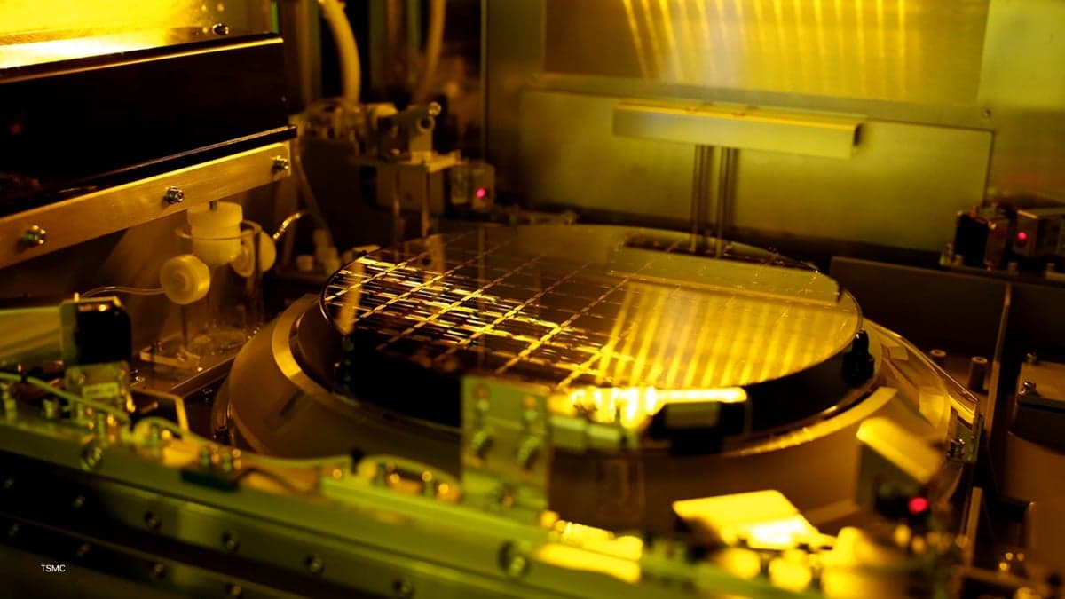
TSMC Uses Nvidia AI to Advance Semiconductor Design and Manufactuing
Companies Mentioned
Why It Matters
Embedding Nvidia AI directly into TSMC’s fabs shortens time‑to‑market and raises yields, reinforcing its lead in advanced‑node production. It also signals a broader shift toward GPU‑based AI across the semiconductor industry.
Key Takeaways
- •TSMC adopts Nvidia CUDA‑X libraries for 20‑50% faster lithography.
- •cuEST GPU library gives TSMC 50× speedup in chemistry simulations.
- •Nvidia H200 GPUs boost fab scheduling, improving productivity.
- •Metropolis AI enhances nanometer‑scale defect detection, reducing re‑labeling.
- •Omniverse FabTwin lets TSMC digitally test fab layouts before build.
Pulse Analysis
The semiconductor sector is confronting unprecedented design complexity as manufacturers push toward sub‑5‑nanometer nodes. Traditional CPU‑based simulations struggle to keep pace with the massive data and physics calculations required for lithography, transistor modeling, and process control. TSMC’s decision to embed Nvidia’s GPU‑accelerated platforms reflects a strategic pivot toward high‑performance AI computing, a trend that mirrors broader industry moves to harness parallel processing for faster, more accurate chip development.
Nvidia’s suite of tools—CUDA‑X, cuLitho, cuEST, cuML, and the H200 GPU family—delivers concrete performance gains for TSMC. Computational lithography sees a 20‑50% reduction in cycle time, while chemistry simulations for material design run up to 50 times faster with cuEST. Machine‑learning‑driven process analytics using cuML trims variation across thousands of fab steps, and GPU‑powered scheduling on H200 GPUs lifts overall fab throughput. In defect inspection, the Metropolis vision AI platform and TAO Toolkit enable nanometer‑scale defect classification with fewer re‑training cycles, directly improving yield.
The partnership’s implications extend beyond TSMC’s own fabs. By showcasing measurable efficiency and yield improvements, the collaboration validates GPU‑centric AI as a viable path for the entire semiconductor ecosystem. It accelerates the adoption of digital twins, such as the Omniverse‑based FabTwin, allowing manufacturers to prototype fab layouts virtually before capital expenditure. As AI‑enhanced manufacturing becomes a differentiator, chipmakers that integrate these capabilities will likely secure a competitive advantage in the race for next‑generation computing power.
TSMC uses Nvidia AI to advance semiconductor design and manufactuing
Comments
Want to join the conversation?
Loading comments...