Unifying III-Vs and Silicon with an RF Interposer
Why It Matters
The interposer eliminates cost and integration barriers between silicon and compound semiconductors, unlocking sub‑terahertz wireless, radar and sensing applications at volume production. It gives manufacturers a CMOS‑compatible route to combine high‑performance III‑V amplifiers with dense digital logic on a single substrate.
Key Takeaways
- •300 mm silicon interposer supports 20‑325 GHz with <0.9 dB/mm loss.
- •XP80 polymer replaces BCB, enabling multilayer routing and lower stress.
- •5 µm RF and 1 µm digital pitches achieve high‑density chiplet integration.
- •Integrated copper pillars and micro‑bumps co‑package InP PA without performance loss.
- •Built‑in thermal sensors ensure reliable high‑power operation up to several watts.
Pulse Analysis
The push toward millimetre‑wave and sub‑terahertz communications has exposed a long‑standing divide: silicon excels at dense digital logic, while III‑V compounds such as InP and GaN deliver unmatched RF power and speed. Traditional packaging forced designers to choose between scalability and performance, limiting system bandwidth and increasing cost. Heterogeneous integration—stacking disparate chiplets on a common substrate—promises to reconcile these trade‑offs, but it requires a platform that can handle ultra‑high frequencies, low loss, and thermal loads without sacrificing manufacturability.
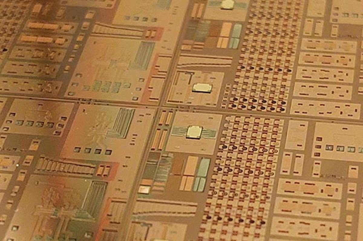
imec’s new RF silicon interposer answers that call. Built on a standard 300 mm low‑resistivity silicon wafer, the stack incorporates three copper redistribution layers and three low‑loss XP80 polymer layers, replacing the earlier BCB dielectric. This architecture achieves insertion losses as low as 0.30 dB/mm at 140 GHz and stays under 0.9 dB/mm even at 325 GHz, rivaling premium glass interposers. With 5 µm RF and 1 µm digital routing pitches, the platform supports dense chiplet placement, while embedded copper pillars and CuNiSn micro‑bumps provide reliable electrical and thermal pathways. Integrated heaters and sensors enable precise thermal management, crucial for high‑power InP and GaN amplifiers that can generate several watts per millimetre of gate width.
The implications for the industry are profound. By delivering a CMOS‑compatible, wafer‑scale solution, the interposer allows foundries to produce mixed‑technology modules at volume, reducing BOM costs and improving yield. Applications ranging from 6G backhaul links and high‑resolution automotive radar to terahertz imaging can now leverage compact, high‑efficiency RF front‑ends without the traditional packaging penalties. As the ecosystem adopts chiplet‑based design, imec’s platform sets a new benchmark for performance, scalability, and thermal reliability, positioning it as a cornerstone for the next generation of wireless and sensing systems.
Unifying III-Vs and silicon with an RF interposer
Comments
Want to join the conversation?
Loading comments...