Why 6.4 Gbps DDR5 Designs Fail and How to Avoid It
Why It Matters
At these speeds a single design flaw can force costly respins, threatening product timelines and margins. Reliable DDR5 PHYs are critical for AI accelerators and industrial SoCs that depend on high‑bandwidth memory.
Key Takeaways
- •DDR5 PHYs above 6.4 Gbps need mandatory equalization
- •Real‑world PCB loss often defeats ideal IBIS‑AMI simulations
- •Low‑jitter PLLs and dynamic delay lines secure timing closure
- •Robust link training and silicon‑proven IP boost mass‑production yield
- •Dual‑channel DDR5 adds synchronization complexity to PHY design
Pulse Analysis
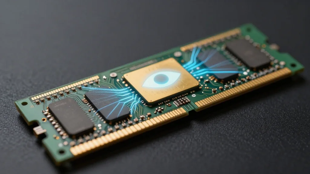
The race to higher memory bandwidth has pushed DDR5 interfaces past the 6.4 Gbps barrier, a regime where copper traces behave like lossy transmission lines rather than simple wires. In this environment, traditional IBIS‑AMI models fall short, and designers must confront the "Glass Weave" effect, PVT variations, and severe impedance mismatches. Companies that ignore these realities risk producing silicon that only works in a lab, not on the production floor, jeopardizing the performance of AI processors, data‑center accelerators, and rugged industrial devices.
Technical success hinges on a multi‑layered PHY strategy. Feed‑Forward Equalization (FFE) pre‑shapes the outgoing signal, while Decision‑Feedback Equalization (DFE) cleans up inter‑symbol interference at the receiver. Power‑integrity measures, such as on‑chip noise suppression, are equally vital because high‑speed switching injects jitter that can collapse the data eye. Low‑jitter PLLs paired with picosecond‑adjustable delay lines provide the timing closure needed for a stable link, and on‑boot link‑training aligns the eye for each board’s unique loss profile. Dual‑channel DDR5 further complicates synchronization, demanding sophisticated digital logic to manage independent sub‑channels and on‑die ECC.
From a business perspective, the cost of a respin far exceeds the expense of proven IP. Leveraging a library of silicon‑validated PHY blocks reduces risk, accelerates time‑to‑market, and ensures consistent yield across foundry lots. Companies like Key ASIC, with over 150 pre‑qualified IPs and a 100 % tape‑out success record, enable customers to focus on system differentiation rather than low‑level analog challenges. This approach not only safeguards margins but also provides the flexibility to meet diverse power and performance targets across AI, automotive, and industrial markets.
Why 6.4 Gbps DDR5 Designs Fail and How to Avoid It
Comments
Want to join the conversation?
Loading comments...