Wooptix Breaks Ground on New Semiconductor Cleanroom Facility
Why It Matters
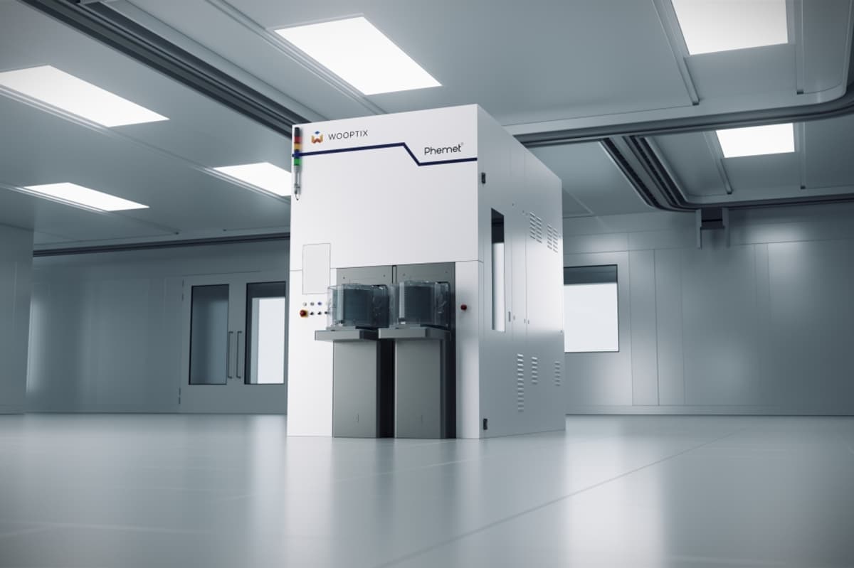
The new cleanroom gives Wooptix greater control over production, accelerating time‑to‑market for its metrology tools while bolstering Europe’s strategic semiconductor supply chain.
Key Takeaways
- •Wooptix breaks ground on 200 m² cleanroom in Tenerife.
- •70 m² cleanroom includes testing and metrology labs.
- •Facility aims for full operation by year‑end 2026.
- •Proximity to sea cuts transport costs for large equipment.
- •Enhances Europe’s semiconductor independence and Spain’s ecosystem.
Pulse Analysis
Semiconductor metrology is a critical enabler for yield improvement and device reliability across the chip manufacturing value chain. Wooptix, a specialist in precision measurement solutions, has leveraged its expertise to address a growing demand for in‑house testing capabilities as fabs adopt advanced nodes. The company's decision to invest in a dedicated cleanroom reflects a broader industry trend where equipment vendors are internalizing R&D and production to shorten development cycles and protect intellectual property. This move positions Wooptix to capture a larger share of the European metrology market.
Tenerife offers a unique blend of logistical and regulatory benefits that align with Wooptix’s operational goals. The island’s port facilities enable direct shipment of large, vibration‑sensitive metrology instruments, cutting freight expenses and reducing handling risk compared with mainland routes. As an EU member, Spain provides access to Horizon‑Europe grants and tax incentives aimed at bolstering high‑tech manufacturing, which can offset a portion of the capital outlay for the 200‑square‑meter plant. Moreover, the growing local tech ecosystem supplies a talent pool versed in photonics and semiconductor processes, supporting rapid scaling.
The Tenerife cleanroom strengthens Europe’s strategic push for semiconductor independence by adding domestic capacity for critical measurement equipment. Customers ranging from research institutes to fab operators will benefit from on‑site validation, shortening the supply chain and improving time‑to‑revenue for new chip designs. As rivals in Asia and the United States continue to dominate wafer‑scale tooling, Wooptix’s localized facility could become a hub for collaborative projects funded by EU innovation programs. In the longer term, the plant may expand beyond metrology, attracting ancillary suppliers and reinforcing Spain’s position as a semiconductor hub.
Wooptix breaks ground on new semiconductor cleanroom facility
Comments
Want to join the conversation?
Loading comments...