X-FAB and Cadence Strengthen Collaboration
Companies Mentioned
Why It Matters
Design migration is a bottleneck for companies upgrading to advanced nodes; this joint solution streamlines the process, helping firms meet performance goals and market deadlines while mitigating supply‑chain and geopolitical pressures.
Key Takeaways
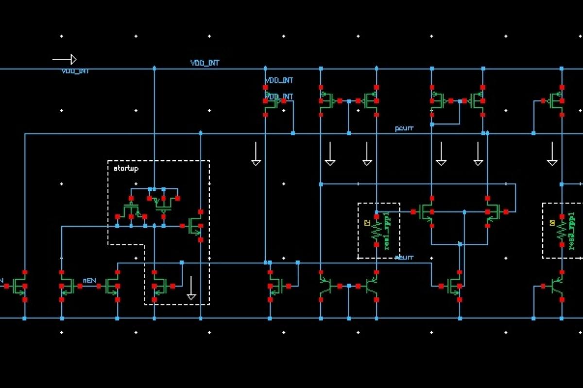
- •Proof of concept migrated designs from 180 nm to 110 nm.
- •Solution supports migration across nodes from 1 µm down to 110 nm.
- •Cadence Virtuoso Studio adds automation for custom IC layout migration.
- •X‑FAB provides dedicated PDK mapping files to preserve performance.
- •Faster migration reduces time‑to‑market and mitigates supply‑chain risks.
Pulse Analysis
As semiconductor manufacturers chase ever‑smaller geometries, the migration of legacy IP becomes a critical hurdle. Moving a design from an older node to a newer one typically requires extensive re‑verification, device‑level tweaking, and layout adjustments, all of which can extend product cycles and inflate costs. The pressure is amplified by volatile supply chains and geopolitical constraints that limit access to cutting‑edge fabs, making efficient migration pathways a strategic priority for maintaining competitiveness.
The X‑FAB‑Cadence partnership addresses these challenges by tightly integrating X‑FAB’s process design kits with Cadence’s Virtuoso Studio migration environment. The combined solution delivers automated re‑optimization, device‑mapping files, and a proven workflow that has already demonstrated a jump from 180 nm to 110 nm. By covering a node range from 1 µm to 110 nm, the offering provides a scalable path for a broad spectrum of customers, from legacy analog designers to those targeting near‑term advanced nodes. The automation reduces manual effort, while the PDK‑specific mapping ensures that critical performance parameters—such as power, speed, and area—are retained.
For the industry, this collaboration signals a maturing ecosystem where EDA vendors and foundries co‑develop migration tools rather than operating in silos. Faster, more reliable migration translates into shorter development timelines, lower R&D expenditures, and a stronger ability to respond to market demand spikes. Companies that adopt the X‑FAB‑Cadence workflow can expect right‑first‑time silicon, improved yield predictability, and a competitive edge in a market where time‑to‑market is often the differentiator. As nodes continue to shrink, such integrated migration solutions will likely become a standard component of semiconductor product strategies.
X-FAB and Cadence strengthen collaboration
Comments
Want to join the conversation?
Loading comments...