MIT News (Quantum Computing) - Latest News and Information
Technology Pulse
EMAIL DIGESTS
Daily
Every morning
Weekly
Tuesday recap
EMAIL DIGESTS
Daily
Every morning
Weekly
Tuesday recap
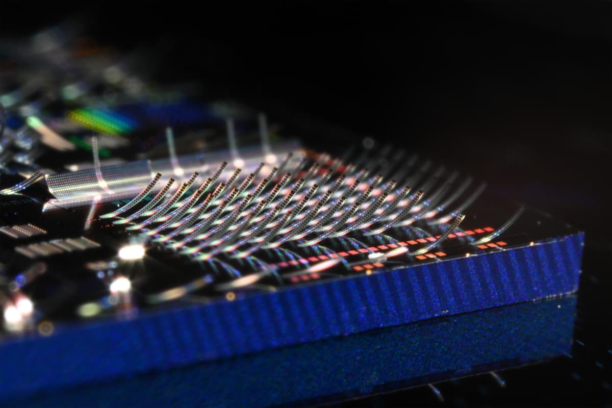
Researchers at MIT, MITRE, Sandia and the University of Arizona have unveiled a photonic chip that uses upward‑curving “ski‑jump” structures to broadcast thousands of individually controllable laser beams into free space. The device leverages a bimaterial strain technique—silicon nitride and aluminum nitride—to form self‑aligned emitters that can project full‑color images at sub‑micron resolution, roughly half the size of a grain of table salt. Demonstrations include ultra‑high‑density pixel arrays and precise steering of laser beams for diamond‑based qubit control. The platform is presented as a scalable bridge between on‑chip waveguides and free‑space optics, opening new possibilities for displays, Lidar and quantum computing.
MIT and MIT Lincoln Laboratory have demonstrated a photonic‑chip based cooling technique that reduces trapped‑ion temperatures to roughly ten times below the conventional Doppler limit. The method uses polarization‑gradient cooling generated by nanoscale antennas on the chip, achieving the cooling...

MIT theorists propose that electrons in certain two‑dimensional materials can fractionalize into anyons, allowing superconductivity to coexist with magnetism. Their calculations show that when 2/3‑charge anyons dominate, they overcome quantum frustration and form a frictionless supercurrent, unlike conventional Cooper‑pair superconductors....