Semiconductor EUV Photoresist Market to Hit $10.8 Billion by 2033
Companies Mentioned
Why It Matters
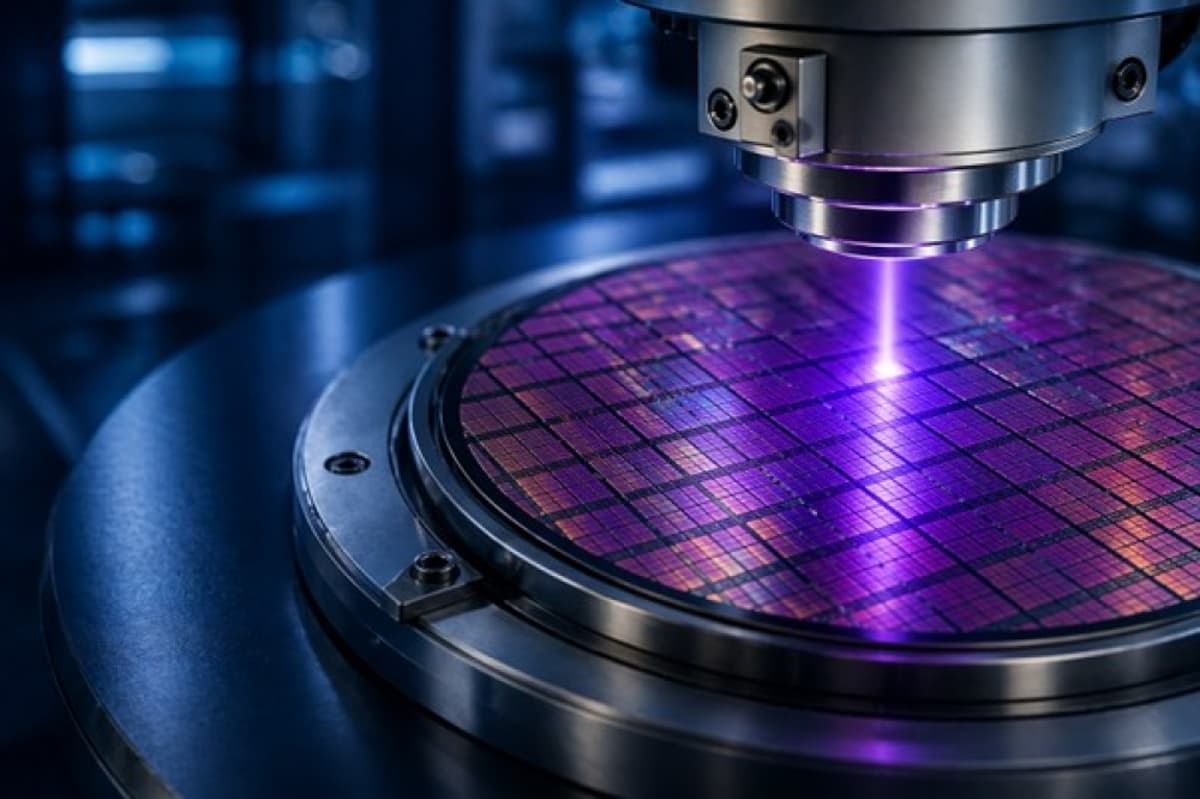
EUV photoresists are essential for producing the next generation of high‑performance chips, making them a strategic bottleneck and growth lever for the semiconductor supply chain. Their market expansion signals deeper investment in advanced lithography, which will shape the pace of AI, cloud, and automotive technology adoption.
Key Takeaways
- •EUV photoresist market projected to reach $10.8 bn by 2033.
- •Advanced nodes below 7 nm drive demand for EUV lithography.
- •AI, data centers, and EVs increase need for high‑precision chips.
- •Metal‑oxide resist chemistry boosts sensitivity and pattern fidelity.
- •High system cost and raw‑material supply constraints limit adoption.
Pulse Analysis
The surge toward sub‑7 nm and sub‑3 nm semiconductor nodes has turned EUV lithography into a production imperative, pushing photoresist demand to unprecedented levels. Chipmakers targeting AI accelerators, hyperscale data centers, and power‑efficient electric‑vehicle processors rely on EUV’s ability to pattern densely packed transistors, translating into a market outlook of $10.8 billion by 2033. This growth is not merely a function of device scaling; it reflects a broader industry pivot toward higher performance per watt, where EUV photoresists become the linchpin for cost‑effective yield improvements.
Technological progress in resist chemistry is narrowing the gap between EUV’s theoretical advantages and practical implementation. Metal‑oxide‑based resists, with superior EUV absorption and reduced line‑edge roughness, are addressing long‑standing challenges such as stochastic defects and photon‑shot noise. Concurrently, refinements to chemically amplified resists enhance sensitivity, allowing lower exposure doses and faster throughput. These material breakthroughs, often born from collaborations between equipment manufacturers and specialty chemical firms, are critical for meeting the stringent resolution and defect‑control requirements of sub‑5 nm patterning.
Despite the upside, the market faces headwinds that could temper its trajectory. The capital intensity of EUV scanners—often exceeding $150 million per unit—and the scarcity of ultra‑pure raw materials create entry barriers that confine adoption to a handful of leading foundries. Competitive dynamics feature entrenched players such as Tokyo Ohka Kogyo, JSR, and DuPont, each vying for differentiation through proprietary formulations and supply‑chain resilience. As the industry pushes toward even finer nodes, the strategic importance of EUV photoresists will intensify, making material innovation and cost‑management pivotal for sustaining the projected market growth.
Semiconductor EUV photoresist market to hit $10.8 billion by 2033
Comments
Want to join the conversation?
Loading comments...