
Closing the Silicon Realization Gap: From Static DFM to Governance for Lifecycle (GFL)
The semiconductor sector has outgrown static Design‑for‑Manufacturing (DFM) sign‑off, which only proves a chip can be fabricated. Modern 2.5D/3D heterogeneous systems encounter substrate warpage, thermal‑current interactions, firmware changes, and aging that can break convergence after tape‑out. The article names this shortfall the Silicon Realization Gap and proposes Governance for Lifecycle (GFL) as a continuous, observability‑driven framework to preserve deterministic behavior throughout a product’s operational life. GFL leverages runtime monitoring, bounded interventions, and fleet‑learning analytics to turn field data into ongoing convergence refinement.

Crossing the Yield Cliff: IDP V6 and the Future of Manufacturing Forecasting
The newly released Industrial Defectivity Prediction (IDP) V6 introduces a two‑layer statistical framework that extends the classic Negative Binomial model to capture “yield cliffs” across nine manufacturing sectors, from semiconductors to pharmaceuticals. By adding an information‑loss correction layer and a threshold‑transition...

CEO Interview with RP Singh of Seasia Infotech
Seasia Infotech, led by co‑founder and CEO RP Singh, has evolved over two decades into a full‑stack digital engineering partner serving startups, enterprises and public‑sector clients worldwide. The firm blends custom software development with AI, cloud, cybersecurity and DevOps to...

CEO Interview with Adi Gelvan of Speedata
Speedata, led by veteran CEO Adi Gelvan, has launched the world’s first Analytics Processing Unit (APU), a silicon‑engineered chip that accelerates SQL‑heavy analytics and AI data‑preparation workloads. The APU promises up to 100× speed gains versus CPUs and GPUs and...
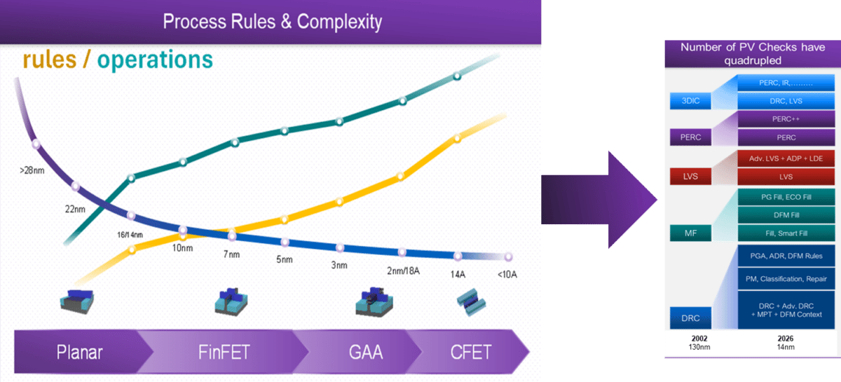
Beyond Tool Interoperability: The Emerging Governed Convergence Problem in Semiconductor Design
The semiconductor sector is moving past tool interoperability toward a "governed convergence" challenge, where specialized tools, domains, and organizations must align to produce manufacturable, high‑performance systems. Fragmentation now spans abstraction layers, physics domains, and decision authority, creating an "entropy wall"...
Panel Discission: Beyond Moore’s Law and the Future of Semiconductor Manufacturing
The semiconductor sector is moving into a post‑Moore’s Law era where transistor shrink alone can no longer deliver performance gains. Panelists highlighted that AI‑driven analytics, massive data pipelines, and intelligent manufacturing ecosystems are becoming essential to improve wafer yields and...

CEO Interview with Dave Kelf, CEO of Breker Verification Systems
Breker Verification Systems reported a 35% revenue increase in 2025, mirroring its 2024 growth, and expects an even stronger 2026 as demand for functional verification accelerates. The company expanded its engineering footprint with a new support facility in Bangladesh and...
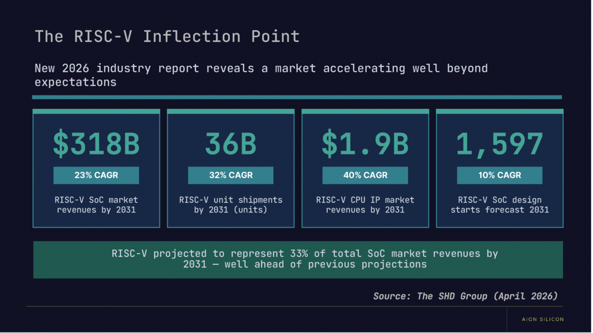
RISC-V: From Niche Architecture to Strategic Foundation
At the RISC‑V Now by Andes conference, Aion Silicon’s CEO Oliver Jones declared that RISC‑V has moved from a niche alternative to a strategic foundation for modern silicon. The company’s experience delivering dozens of 7 nm and smaller designs shows the...

Bringing Mathematical Rigour in the World of Hardware – a Journey Into Formal Verification
Robert Simpson, a mathematics graduate, joined Axiomise to apply formal verification (FV) to silicon design. He describes how rigorous logical reasoning uncovers bugs that conventional testing misses and how his academic habits translate to real‑world hardware correctness. At Axiomise, he...

The Great Divide: A Tale of Three Hardware Emulation Architectures
Hardware emulation, born in the 1980s to bridge the gap between slow gate‑level simulation and late silicon prototypes, has split into three architectural families: processor‑based, custom‑FPGA‑based, and commercial‑FPGA‑based. Processor‑style platforms, pioneered by Quickturn and later Cadence, deliver deep visibility but...
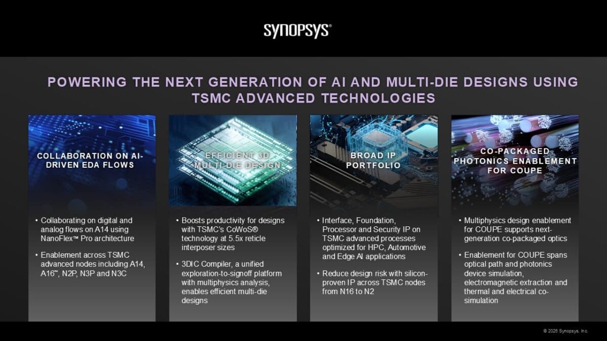
Synopsys and TSMC Deepen AI Design Alliance: What It Means
Synopsys and TSMC announced an expanded AI design alliance that couples silicon‑proven IP, AI‑driven EDA flows, and advanced packaging for 3 nm and emerging 2 nm nodes. The partnership adds 64 G UCIe and 224 G high‑speed interconnect IP, agentic run assistance in the...
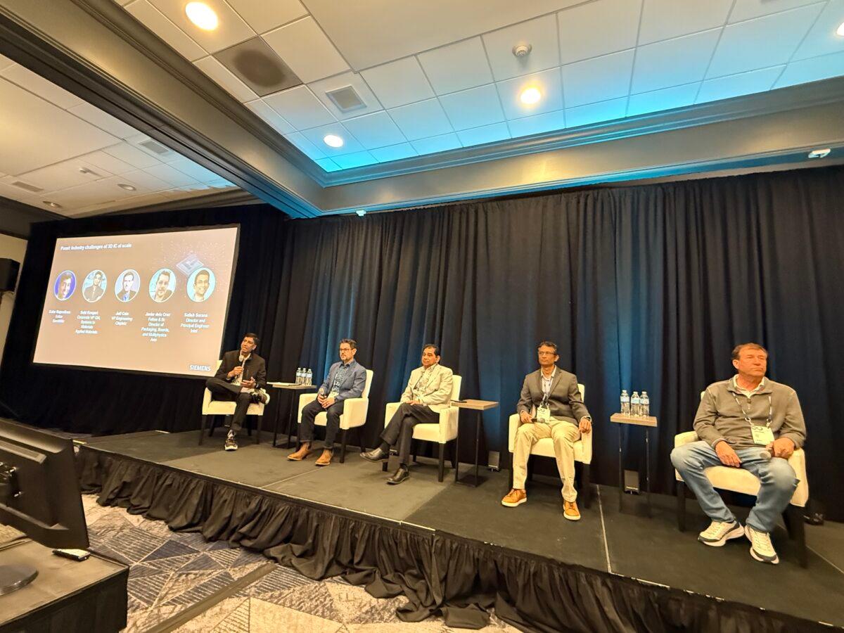
Siemens U2U 3D IC Design and Verification Panel
Siemens convened a panel of industry experts to discuss the shift from 2D chips to 3D ICs and chiplet architectures. The discussion highlighted how stacking multiple dies improves performance, power efficiency, and bandwidth for AI, HPC, and data‑center workloads. Panelists...
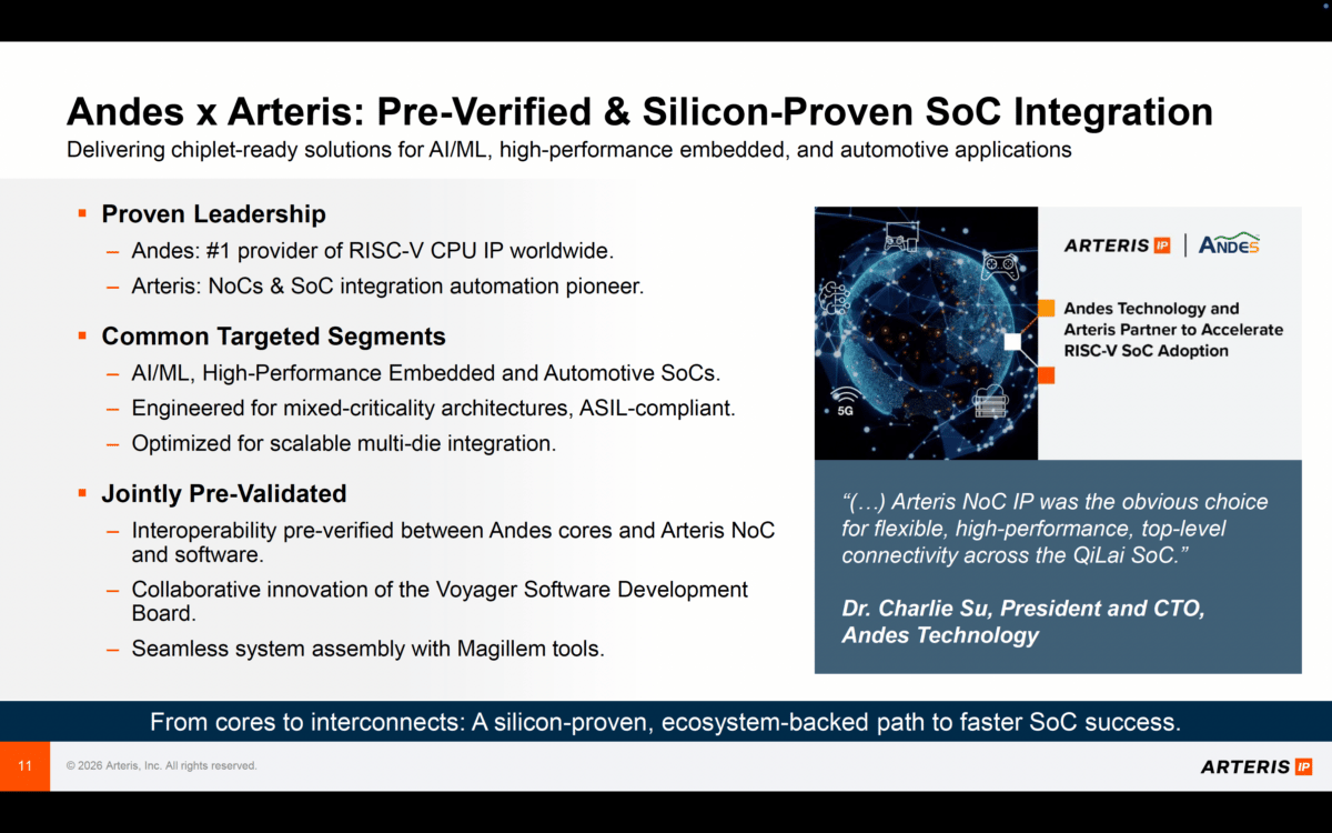
Connecting the Dots: Why RISC-V System Design Is Entering a New Era
At the recent RISC‑V Now event, Andes and Arteris highlighted that the architecture’s future depends on system‑level design rather than just ISA advantages. Modern SoCs are becoming heterogeneous, with data movement now the dominant energy and performance bottleneck. Effective Network‑on‑Chip...

Rethinking ECAD IT Infrastructure: From Fragmentation to an Engineering Platform
The semiconductor sector is confronting unprecedented design complexity driven by advanced nodes, heterogeneous integration, and AI‑enhanced workflows, exposing a critical gap in ECAD IT infrastructure. Traditional build‑it‑yourself models force companies to allocate extensive resources to custom DevOps, licensing, and orchestration,...

CEO Interview with Geoffrey Rodgers of Chameleon Semiconductor
Chameleon Semiconductor, led by CEO Geoffrey Rodgers, provides a soft embedded FPGA (eFPGA) IP fabric delivered as synthesizable RTL, allowing post‑silicon programmability in ASICs and SoCs. The company targets a "design‑for‑change" model, letting customers update functionality after tape‑out and avoid...

Bronco AI Webinar: Full-Chip SoC Debug in 15 Minutes
Bronco AI’s new platform promises to cut full‑chip SoC debug cycles from days to under 15 minutes by leveraging large‑scale AI reasoning models integrated with a proprietary EDA stack. The system automatically gathers logs, waveforms, code and specifications at regression...

Solving the EDA Tool Fragmentation Crisis
The Calibre Connectivity Interface (CCI) converts LVS verification data into a universal, queryable database, allowing diverse EDA tools to share accurate design information without manual translation. By tapping the Standard Verification Database, CCI feeds parasitic extraction, power‑integrity, electromagnetic, and soft‑error...
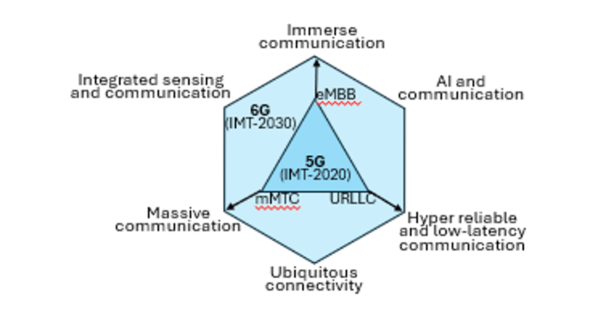
Advanced Microelectronics Paving the Way for 6G with Alphacore
The telecom ecosystem is already laying the groundwork for sixth‑generation (6G) mobile networks, guided by the ITU’s IMT 2030 framework and early 3GPP study items. 6G aims to exploit sub‑terahertz spectrum, massive phased‑array antennas, and AI‑embedded air interfaces, demanding semiconductor breakthroughs...

WAVE-N Specialized Video Processing NPU for Edge AI Systems
Chips&Media unveiled the WAVE‑N specialized video‑processing NPU to meet the growing demand for high‑performance, low‑power AI inference on edge devices. The accelerator combines massive parallel compute, on‑chip memory buffers, and dedicated tensor units to speed up computer‑vision workloads such as...

Complex PCB Signoff Challenges
Siemens’ HyperLynx DRC tool introduces rule‑based, automated electrical verification for complex printed‑circuit‑board (PCB) designs that carry high‑speed protocols such as USB, PCIe, DDR and HDMI. The solution replaces time‑consuming manual inspections with continuous, scriptable checks that flag signal‑integrity, power‑integrity, EMI/EMC...

User Experience and Control in Agentic Systems. Innovation in Verification
This month’s discussion pivots from merely linking tools, agents and orchestration toward foundational principles for building effective agentic systems. Speakers such as Paul Cunningham, GM of Verification at Cadence, emphasized the importance of user experience and seamless human‑in‑the‑loop integration. The...

Scalable Network-on-Chip Enables a Modular Chiplet Platform
Menta has launched the MOSAICS platform, a modular chiplet architecture that uses a Known Good Die hub to orchestrate communication among heterogeneous components. The hub relies on Arteris' FlexNoC interconnect, which can handle more than 30 initiators and targets at...

All in One Bluetooth Audio: A Complete Solution on a TSMC 12nm Single Die
The SemiWiki webinar "All‑in‑One Bluetooth Audio: A Complete Solution on a TSMC 12 nm Single Die" showcases a fully integrated Bluetooth audio system built on TSMC’s 12 nm process. By consolidating RF front‑end, baseband, DSP, memory and power management onto one die,...

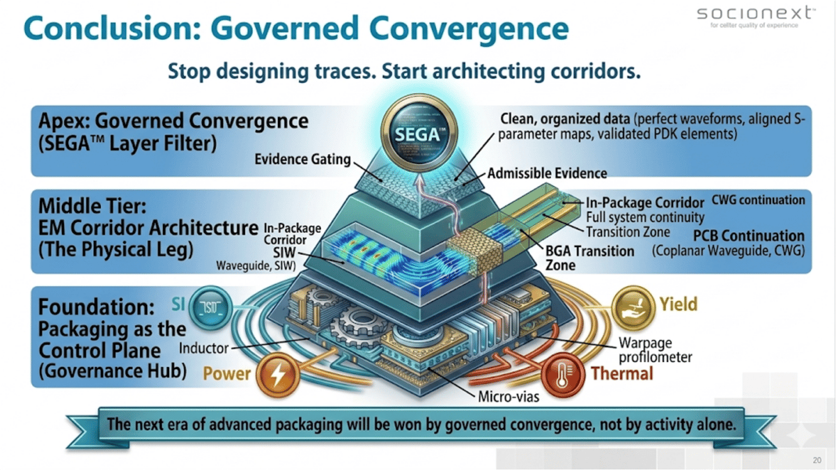
Closing the Reality Gap: A New Architecture for 1.8-Tb/s Chiplet Governance
Senior Lead Architect Dr. Moh Kolbehdari of Socionext unveiled the SEGA™ (Systematic Engineering Governance Architecture) framework to close the “Reality Gap” between simulation and high‑volume manufacturing for 1.8‑Tb/s chiplet interconnects. SEGA™ positions the package as an Active Control Plane, introduces...

CEO Interview with Xianxin Guo of Lumai
Lumai, an Oxford University spin‑out, is commercialising optical computing technology to accelerate AI inference in data centres. CEO Xianxin Guo says the hybrid optical‑electronic processor replaces power‑hungry electronic tensor operations with light‑based computation, delivering dramatically higher performance‑per‑watt. The company targets...

Two Paths for AI in Semiconductor Manufacturing: Platform Integration Vs. Point Solutions
AI is becoming a core layer in semiconductor fabs as data volumes explode, prompting two distinct adoption pathways. In North America and Europe, vendors pursue platform‑scale AI that integrates with legacy systems and supports multiple use cases, while Chinese fabs...

Carbon in the Age of AI Chips: What the Semiconductor Industry Needs to Know This Earth Day
TechInsights released its Earth Day sustainability report, "Carbon in the Age of AI Chips," highlighting a surge in semiconductor emissions as AI demand accelerates. Fabrication emissions are projected at 186 million metric tons CO₂e in 2026, climbing to 247 million by 2030,...
Could Neutral Atoms Take the Lead in Quantum Computing?
A new pre‑print from Oratomic proposes that neutral‑atom quantum computers, which use laser‑tweezed atoms as qubits, could outpace traditional superconducting platforms. The key innovation is dynamic reconfigurability, allowing qubits to be moved into proximity for two‑qubit gates, which dramatically lowers...

Transitioning Voltage Regulator Design From Unidirectional To Bidirectional
The article by Nazzareno Rossetti outlines the shift from traditional unidirectional voltage regulators to bidirectional converters, a change driven by modern energy‑management systems that must move power between electric vehicles, photovoltaics, home batteries, and the grid. It highlights how synchronous...
How to Overcome the Advanced Node Physical Verification Bottleneck
Synopsys unveiled its IC Validator platform as a new answer to the mounting physical‑verification bottlenecks that accompany advanced‑node designs. The tool’s HyperSync distributed‑processing engine delivers 2‑4× faster full‑chip antenna and PERC ESD checks while slashing CPU usage by up to 70 %. Elastic...

Is Intel About to Take Flight?
Intel announced a strategic partnership with Elon Musk to supply custom AI inference chips for Tesla, SpaceX and other ventures, leveraging its under‑utilized Hillsboro fab that already houses ASML EUV equipment. The deal offers Musk a queue‑free production line while...

WEBINAR: Intrinsic Techniques in RF Power Amplifier Design
Keysight’s second RF Power Amplifier Design master‑class webinar dives into intrinsic modeling techniques for GaN transistors, complementing traditional load‑pull methods. The session showcases a Class J PA built around an intrinsic‑node model, demonstrating how waveform engineering and Fourier‑based impedance mapping boost...
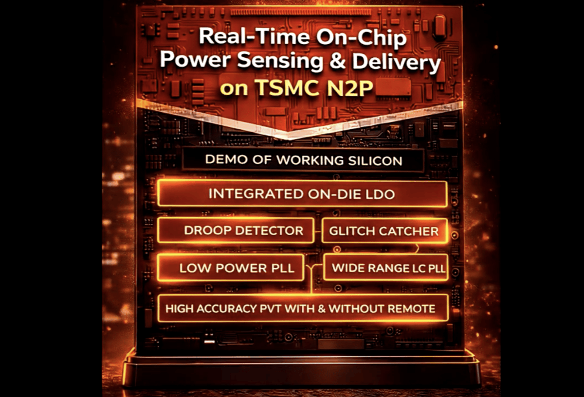
Analog Bits Demos Real-Time On-Chip Power Sensing and Delivery on N2P at the TSMC 2026 Technology Symposium
Analog Bits demonstrated a suite of real‑time on‑chip power‑sensing and delivery IP at the TSMC 2026 Technology Symposium, running on the company’s N2P test chip. The portfolio includes an on‑die LDO with 30% area reduction, droop detector, glitch catcher, ultra‑low‑power...
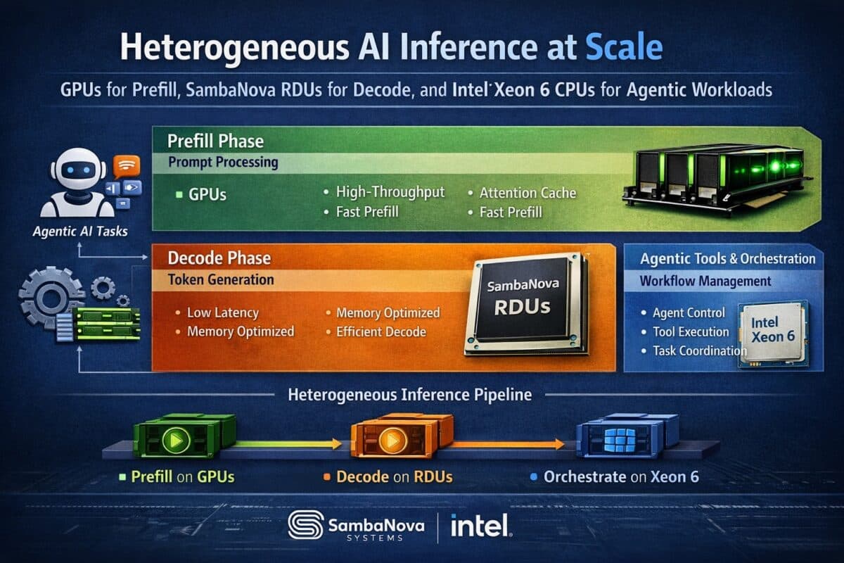
Disaggregating LLM Inference: Inside the SambaNova Intel Heterogeneous Compute Blueprint
Intel and SambaNova announced a heterogeneous inference blueprint that assigns distinct phases of large‑language‑model serving to the most suitable hardware. GPUs accelerate the parallel prefill stage, while SambaNova’s Reconfigurable Dataflow Units (RDUs) handle the memory‑bound decode phase. Intel Xeon 6 CPUs...

CEO Interview with Johan Wadenholt Vrethem of Voxo
Voxo, founded in Stockholm in 2016, uses AI to capture and transform live event speech into branded, shareable content within minutes. After a successful pilot at Techarena 2024, the company pivoted to event‑focused analytics, now serving global enterprises such as...
WEBINAR: Beyond Moore’s Law and The Future of Semiconductor Manufacturing Intelligence
The SemiWiki webinar on April 23 2026 gathered leading AI, EDA and fab executives to discuss how semiconductor manufacturing is moving beyond Moore’s Law. Speakers highlighted AI‑driven digital twins, predictive metrology, agentic AI and generative design as tools to tame the complexity...

Speculation: Silicon’s Most Expensive Compulsion
Modern high‑performance CPUs devote 30‑50% of die area and up to 30% of dynamic power to out‑of‑order speculative execution hardware that rarely benefits AI, scientific and EDA workloads. Simplex Micro’s Time‑Based Scheduling (TBS) removes most speculation structures from the vector...

Exploring the Hidden Complexity of Modern Power Electronics Design – A Siemens White Paper
Siemens released a white paper detailing the hidden complexity of power‑delivery‑network (PDN) design in modern power electronics. It outlines four primary failure mechanisms—improper PCB stack‑up, capacitor aging, thermal/mechanical stress, and out‑of‑spec component use—and shows how they erode voltage stability and...

Effective Defense Against Hacks at the Edge
PQShield unveiled its MicroCore IP, a post‑quantum security suite that fits within as little as 5 KB of SRAM for edge‑device IoT applications. The offering covers secure boot, post‑quantum TLS, and side‑channel‑resistant cryptography, all deliverable as software‑only updates or with optional...

Hardening the Silicon: Why Analog Anti-Tamper IP Is the New Security Baseline
Analog anti‑tamper IP is emerging as a baseline for hardware security as billions of IoT and automotive SoCs face increasingly sophisticated physical attacks. Hackers now employ fault injection, glitching, side‑channel, and micro‑probing techniques that can bypass software‑only protections and compromise...

Renesas Scalable Automotive SoC Design Using Arteris NoC
Renesas has integrated Arteris FlexNoC interconnect IP into its next‑generation Gen‑5 R‑Car automotive SoCs. The NoC fabric links Arm CPU clusters, GPUs and neural‑processing accelerators, delivering scalable bandwidth and deterministic QoS for advanced ADAS and autonomous‑driving workloads. Power consumption drops...

Calibrating Quantum Computing Activity in Financial Services
At a Fujitsu‑hosted event, senior technologists from Fujitsu, HSBC and industry analysts discussed the realistic state of quantum computing in financial services. The consensus was that while quantum offers promise for probabilistic modeling, optimization and quantum‑machine‑learning, hardware is still years...

NoC Matters: Designing the Backbone of Next-Gen AI SoCs
The article argues that network‑on‑chip (NoC) design has become the cornerstone of modern AI‑centric System‑on‑Chips, dictating performance, power efficiency, and scalability. As heterogeneous accelerators proliferate, data movement dominates system behavior, making NoC topology, buffering, and QoS policies critical. Designers must...

From Wooden Boards to White Gloves: How FPGA Prototyping and Emulation Became Two Worlds of Verification… and How the Convergence...
FPGA prototyping and hardware emulation originated from parallel needs—speed and system realism versus deep debugging of ever‑larger designs. Prototyping leverages re‑programmable silicon to run software workloads early, while emulation provides controlled, observable execution for complex verification. Historically served distinct vendor...
CEO Interview with Dr. Hardik Kabaria of Vinci
Vinci, led by founder‑CEO Dr. Hardik Kabaria, has deployed the first production‑grade physics foundation model that continuously computes thermal and mechanical behavior directly on semiconductor geometry. The deterministic, solver‑accurate platform replaces episodic simulation with an always‑on engine, delivering up to...

CEO Interview with Steve Kim of Chips&Media
Chips&Media CEO Steve Kim highlighted that the Seoul‑based multimedia IP firm powers more than 3 billion devices for over 150 top‑tier customers. The company’s portfolio now spans high‑efficiency 8K video codecs, AI‑focused image‑processing NPUs and advanced Frame Buffer Compression (FBC) technology....

YieldHUB Expands Its Impact with New Technology and a New Website
YieldHUB has launched a redesigned website and introduced YieldHUB Live, a real‑time manufacturing intelligence layer for semiconductor test floors. The new portal groups solutions by product lifecycle, device architecture and user role, while the live platform delivers continuous visibility, anomaly...

NXP Expands Arteris NoC Deployment to Scale Edge AI Architectures
NXP announced an expanded deployment of Arteris’s NoC and cache‑coherent IP suite—including FlexNoC®, Ncore®, CodaCache® and the Magillem® integration platform—across its upcoming edge‑AI silicon. The move targets the growing need for deterministic latency, high bandwidth, and safety‑critical isolation in heterogeneous...

Architecting Intelligence: The Rise of RISC-V CPUs in Agentic AI Infrastructure
SiFive announced a $400 million Series G round that lifts its valuation to $3.65 billion, earmarked for next‑generation RISC‑V CPU IP aimed at agentic AI data‑center workloads. The funding will accelerate hardware co‑design that tightly integrates scalar, vector and matrix compute units to...

Intel, Musk, and the Tweet That Launched a 1000 Ships on a Becalmed Sea
Intel announced a partnership with Elon Musk’s Terafab project, joining SpaceX, xAI and Tesla to develop a 1‑terawatt‑per‑year AI compute fab. The deal follows Intel’s $11.1 billion federal rescue, converting unspent grants into a 9.9% U.S. government equity stake. Musk’s ecosystem...