
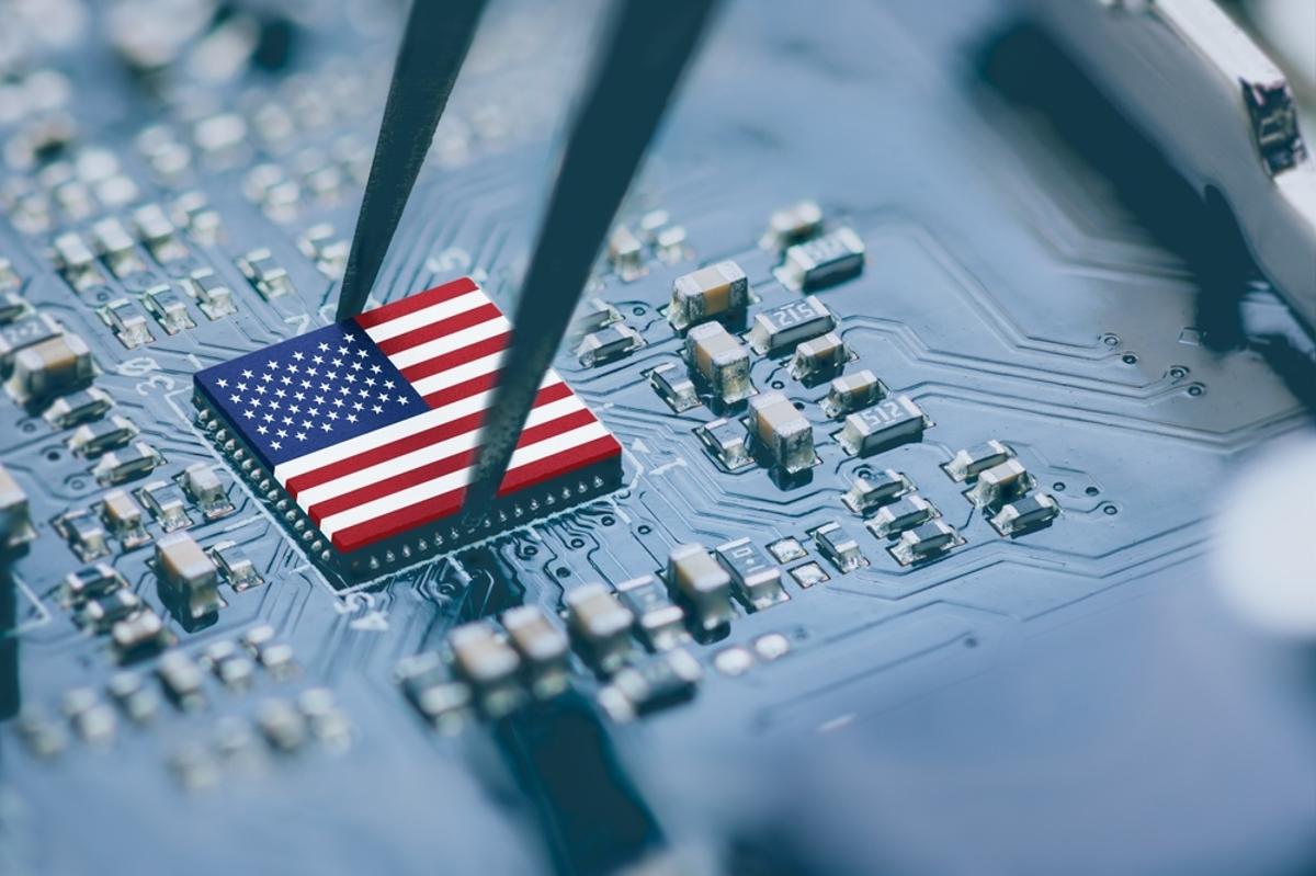
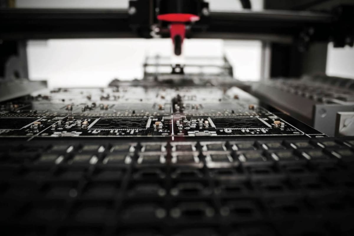
AMD to Invest $10 Billion+ in Taiwan
AMD announced a commitment of over $10 billion to expand its Taiwan ecosystem, targeting advanced packaging and AI‑focused silicon manufacturing. The funding will accelerate development of Elevated Fanout Bridge (EFB) interconnects and support the Helios rack‑scale AI platform slated for the second half of 2026. Partnerships with local ODMs and packaging firms aim to boost performance, efficiency and volume production of next‑generation AI infrastructure. The move strengthens AMD’s supply chain amid global chip competition and geopolitical tensions.
Quantum Technology Solutions to Scale US Quantum Manufacturing
GlobalFoundries has launched Quantum Technology Solutions, a dedicated quantum manufacturing business backed by a $375 million letter of intent from the U.S. Department of Commerce. The initiative leverages GF’s FDX™ cryogenic CMOS platform and advanced packaging to produce quantum processor units...
X-FAB and Cadence Strengthen Collaboration
X‑FAB and Cadence have expanded their partnership to deliver a joint design‑migration solution that couples X‑FAB’s process‑specific PDKs with Cadence’s Virtuoso Studio automation tools. The offering enables customers to move designs from older CMOS nodes to newer geometries quickly, with a...

Arteris Technology Adopted by Li Auto for Intelligent Vehicles
Li Auto has integrated Arteris’s FlexNoC 5 network‑on‑chip IP and Magillem integration automation into the proprietary SoC powering its new L9 Livis SUV. The SoC delivers 2,560 TOPS of AI compute, supporting autonomous driving, ADAS, and immersive in‑vehicle experiences. Arteris’s technology enables efficient...

Semidynamics and SiPearl to Develop EU-Sovereign Rack-Scale AI Compute Platform
Semidynamics and SiPearl announced a joint effort to build a European‑sovereign, rack‑scale AI compute platform that pairs SiPearl’s Arm‑based CPU with Semidynamics’ RISC‑V AI inference ASIC. The system will adhere to Open Compute Project standards, delivering high density, performance‑per‑watt and...
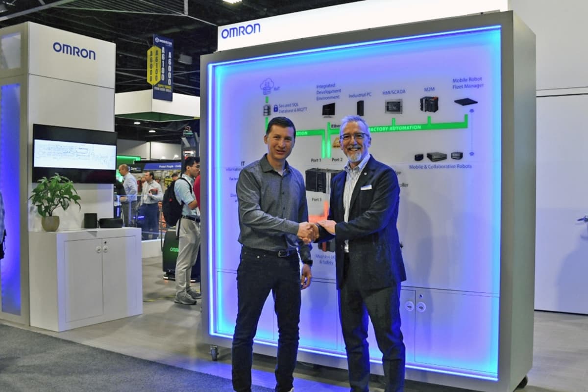
Comau and Omron Robotics to Collaborate
Comau and Omron Robotics have signed a strategic collaboration to accelerate advanced industrial automation adoption worldwide. The partnership targets high‑growth sectors such as electronics, semiconductors, medical manufacturing, and light‑industrial intralogistics. By merging Comau’s robotics hardware with Omron’s control and software...

JST Enhances Applications Lab
JST has upgraded its Applications Lab with the Ospray Single Wafer Wet Processing System, an enhanced Front Linear Automated (FLA) Bench featuring an STG Apex dryer, and a suite of new metrology tools. The new equipment supports wafer sizes up...
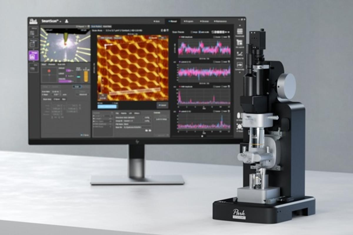
Park Systems Launches NX1
Park Systems has launched the NX1 atomic force microscope, developed with Prof. Franz J. Giessibl of the University of Regensburg. The NX1 translates the ultra‑high‑vacuum atomic‑resolution capability of the Orpheus II prototype into a commercial instrument for ambient labs. It features...
The Semiconductor Industry Is Set to Surpass $1 Trillion by 2030, Driving Industry Innovation
The global semiconductor market posted a record $791.7 billion in 2025, a 25.6% jump, and is projected to top $1 trillion by 2026. Growth is driven by AI, data centers, 5G/6G, electric vehicles and edge computing. Marco Van Der Haar of Malvern...
Chip-Processing Method Could Assist Cryptography Schemes to Keep Data Secure
MIT engineers unveiled two low‑cost hardware innovations that could reshape security and computing at the edge. First, they devised a twin physical‑unclonable‑function (PUF) fabrication method that splits a chip so each half shares a unique fingerprint, enabling direct authentication without...
CEA-Leti and NcodiN Partner to Industrialise 300 Mm Silicon Photonics
CEA‑Leti announced a series of strategic collaborations aimed at scaling next‑generation silicon photonics and memory technologies. In partnership with French startup NcodiN, the institute will transfer the company’s nanolaser‑enabled optical interposer to a 300 mm silicon‑photonic process, targeting sub‑0.1 pJ/bit links for...

Unlocking Yield Improvements in Advanced Packaging Through Materials-Driven Failure Analysis
Advanced packaging—3D ICs, FOWLP, chiplets—now underpins AI, 5G, and edge computing, but its complex material interfaces are creating severe yield pressure. Traditional defect inspection alone cannot capture the subtle, multiscale failures that arise from thermal stress, CTE mismatch, and contamination....

Optimising SiCr Deposition for High-Yield Bipolar-CMOS-DMOS Manufacturing with Picosecond Ultrasonics
Picosecond ultrasonic (PULSE™) technology provides non‑contact, sub‑angstrom thickness metrology for silicon‑chromium (SiCr) films used in bipolar‑CMOS‑DMOS (BCD) devices. The technique, validated against TEM, achieved repeatability better than 0.5 Å (1σ) and captured wafer‑wide uniformity across 49 points. Simultaneously, reflectivity measurements revealed...
Shifting Supply Chains in the Era of Photonics
The article titled “Shifting supply chains in the era of photonics” appears to be unavailable, offering only a 404 error page. Nonetheless, the headline signals a growing focus on how photonics manufacturers are re‑engineering their supply chains amid component shortages,...
Beyond High-NA EUV: Particle Accelerator Technology Promises Exciting Future for Lithography
TAU Systems CEO Jerome Paye proposes compact laser‑wakefield acceleration (LWFA) free‑electron laser sources to replace traditional EUV lithography. High‑NA EUV is hitting both physical and economic limits, prompting a search for brighter, tunable light. LWFA can deliver orders‑of‑magnitude higher photon...