MIT Lincoln Lab Buys Aixtron Hyperion 300mm MOCVD Systems
MIT Lincoln Laboratory has purchased two Aixtron Hyperion 300 mm metal‑organic chemical vapor deposition (MOCVD) systems under a partnership backed by the Massachusetts Governor’s Office and the Northeast Microelectronics Coalition (NEMC). The tools will be installed at the lab, primarily configured for 200 mm wafers but capable of handling 300 mm substrates, enabling flexible research across wafer sizes. One system will focus on gallium nitride (GaN) power and RF device development, while the second will support two‑dimensional (2D) materials research such as next‑generation transistors. The acquisition is part of NEMC’s SCALE Capital Program aimed at accelerating domestic semiconductor innovation.
Nanjing-Based Casela to Buy $25.4m of InP Wafers From AXT’s Tongmei During 2027
Nanjing‑based Casela Technologies has signed a long‑term supply agreement with AXT Inc.’s Beijing Tongmei Xtal Technology to purchase indium phosphide (InP) wafer substrates worth RMB 173 million (≈US$25.4 million) in 2027. The deal obligates Casela to pre‑pay half the amount within 15 business...
Coherent to Receive $50m US CHIPS Act Funding to Expand Sherman 6-Inch InP Fab
Coherent Corp will receive up to $50 million in CHIPS Act funding to expand its 6‑inch indium phosphide (InP) photonic fab in Sherman, Texas. The expansion will double production space, quadruple wafer capacity, and create more than 1,000 jobs, including 550...
JX Expanding InP Substrate Production Capacity Again to Meet Data-Center Optical Communications Demand
Tokyo‑based JX Advanced Metals announced a new four‑year investment of up to ¥120 bn (approximately $800 million) to expand its indium phosphide (InP) substrate production. The plan adds a new facility in Hitachinaka, Ibaraki, boosting capacity by 7‑10 times beyond the existing Isohara...
Enkris Unveils High-Speed, Low-Power Micro-LED Optical Interconnect Product
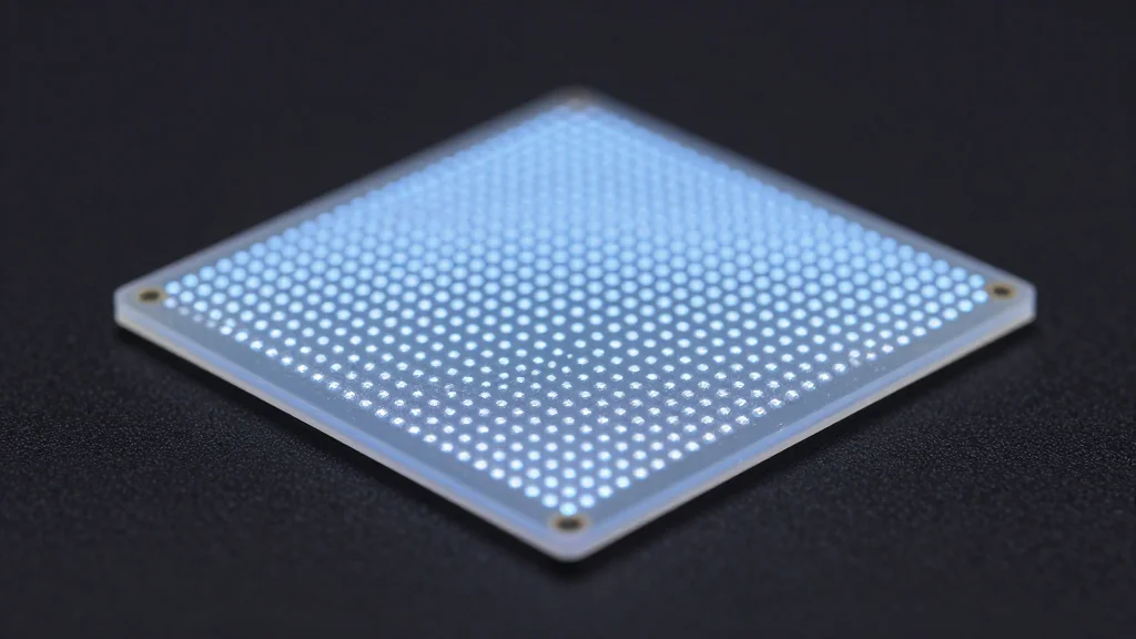
Enkris Semiconductor announced a new micro‑LED optical interconnect product built on 8‑inch and 12‑inch GaN‑on‑silicon wafers. The device delivers a 3 dB bandwidth of 1.6 GHz while operating at a modest 500 A/cm², consuming less than 1 pJ per bit. By suppressing the quantum‑confined...
Element Six and Orbray Accelerate Wafer-Scale Single-Crystal Diamond for Volume Production
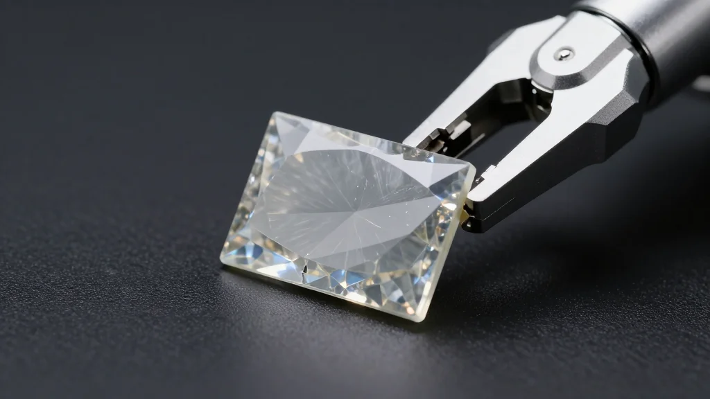
Element Six and Japan’s Orbray announced a reproducible 3‑inch wafer‑scale single‑crystal diamond (WSC) process, marking a leap in size, uniformity and manufacturability. The partnership is also advancing 4‑inch substrates and preparing 2‑inch wafers for epitaxial and thermal‑bonding applications at Element...
PicoJool Introduces 200G VCSELs for Scale-Up AI Data Centers
PicoJool Inc., a Palo Alto‑based optical‑chip maker, announced 200 G VCSELs that exceed 37 GHz bandwidth for hyperscale AI data centers. The company will begin sampling chip‑level products in Q3 2026, including quad‑100 G, quad‑200 G and 32 × 50 G NRZ micro‑VCSELs. Leveraging a manufacturing partnership with...
NUBURU Agrees Lyocon-Led Alliance with SunCubes
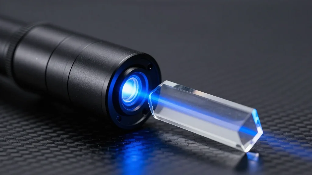
NUBURU Inc. has signed a binding head‑of‑terms agreement with Italy’s SunCubes, channeling the partnership through its laser‑technology subsidiary Lyocon. The deal includes a staged strategic investment of up to €1 million (≈ $1.1 million), with an initial €250,000 advance and a second €750,000...
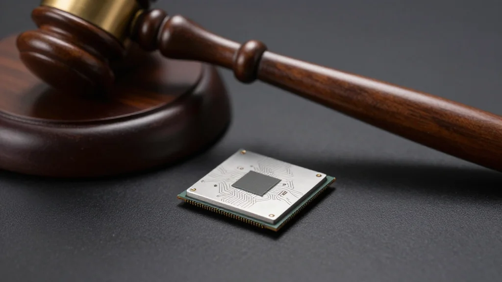
China’s Supreme Court Upholds Injunction Against Infineon, Says Innoscience
China's Supreme People’s Court issued a final review decision upholding a lower‑court injunction that bars Infineon Technologies from selling its gallium nitride (GaN) power chips in mainland China. The ruling confirms Infineon infringed two core Innoscience patents and orders an...
Volta Metals Awarded up to $500,000 From Ontario’s Critical Minerals Innovation Fund
Volta Metals Ltd received a maximum grant of $500,000 CAD (≈$365,000 USD) from Ontario’s Critical Minerals Innovation Fund to fund metallurgical and processing work at its Springer Rare Earth Element and Gallium Project. The award covers up to 50 % of eligible...
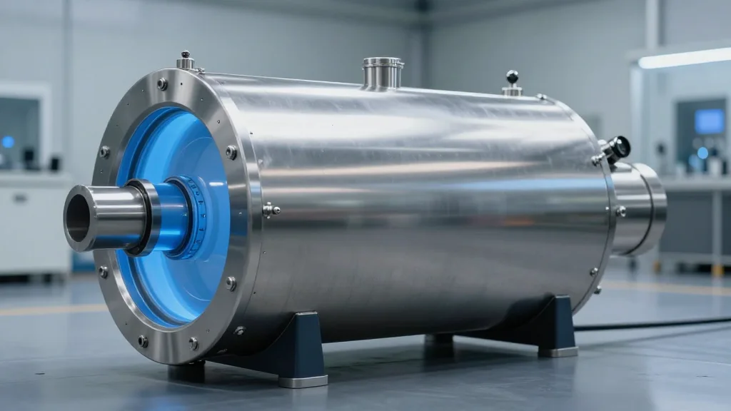
Veeco’s New LUMINA+ MOCVD System Qualified by Ennostar
Veeco Instruments announced that Ennostar Corp qualified its new LUMINA+ metal‑organic chemical vapor deposition (MOCVD) system for high‑volume arsenide and phosphide production. The platform, built on TurboDisc technology, features the industry’s largest‑capacity reactor and promises breakthrough productivity. Ennostar will deploy...
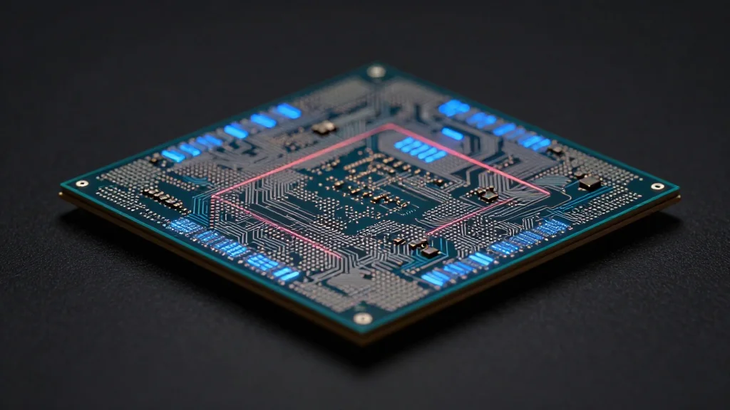
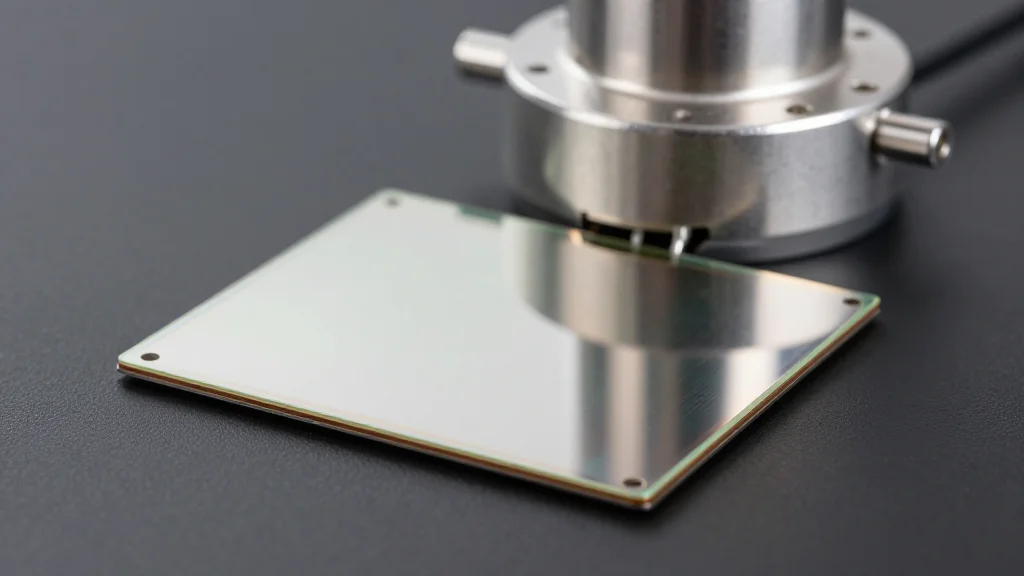
Imec Adds High-Density MIMCAPs, Passive Modeling and Laser-Assisted Bonding to 300mm RF Silicon Interposer Platform
Imec has upgraded its 300 mm RF silicon interposer platform with high‑density MIM capacitors, a scalable passive‑component modeling framework, and laser‑assisted bonding for III‑V chiplet assembly. The new MIMCAP design delivers 10‑to‑100× higher capacitance density, while the modeling tool accurately predicts...
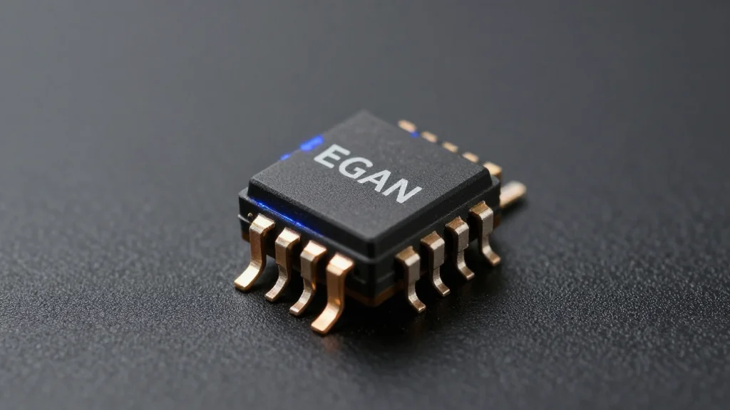
EPC2378 25V, 410µΩ eGaN Enters Mass Production for High-Density DC–DC Conversion
Efficient Power Conversion (EPC) announced that its EPC2378 25 V eGaN power transistor is now in mass production. The device offers a best‑in‑class 410 µΩ typical R_DS(on) and a low R_DS(on)×Q_G figure of merit, supporting up to 101 A continuous current in a...
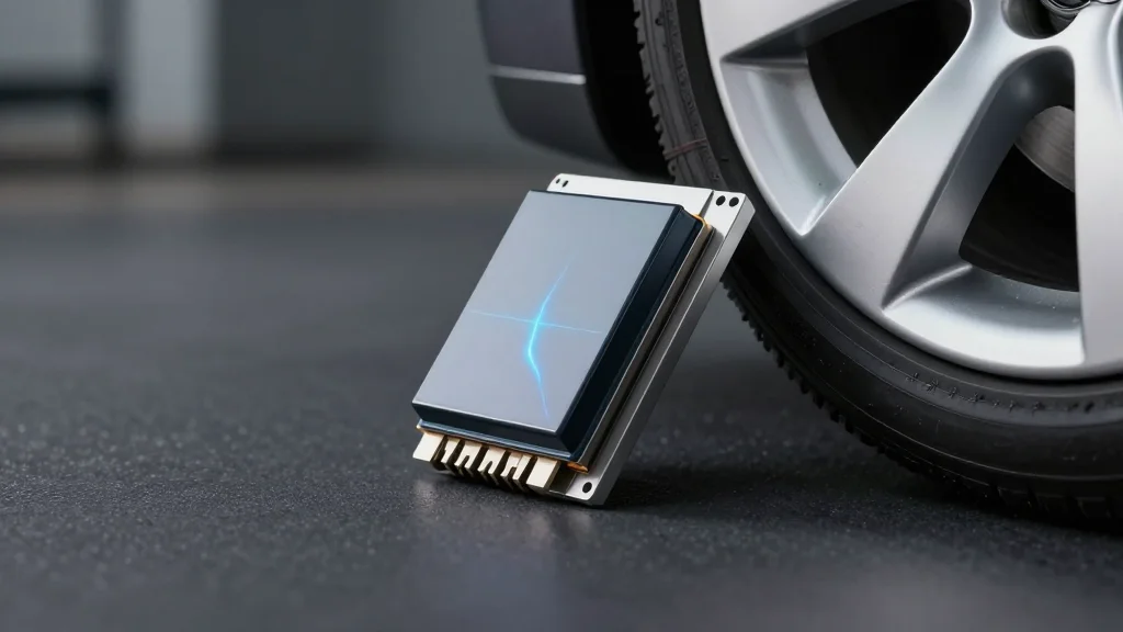
Wolfspeed Introduces Gen 5 SiC MOSFET Technology
Wolfspeed unveiled its fifth‑generation silicon‑carbide (SiC) MOSFET platform, Gen 5, targeting 1200 V and 750 V automotive and industrial power modules. The new devices cut specific on‑resistance by up to 27% versus competing 5 mm × 5 mm SiC parts and raise continuous junction temperature capability to...
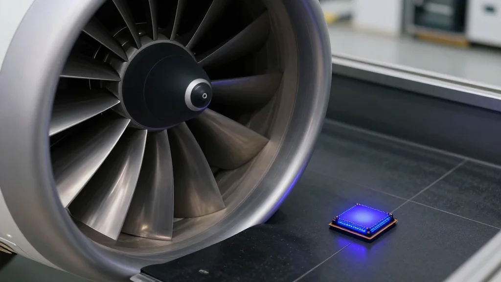
GE Aerospace and Wolfspeed Sign MoU to Collaborate on Accelerating High-Voltage Silicon Carbide Adoption
GE Aerospace and Wolfspeed have signed a memorandum of understanding to accelerate high‑voltage silicon carbide (SiC) adoption across aerospace, defense, and industrial markets. The partnership will develop standards for SiC‑based power modules, enabling solid‑state transformers and more compact, efficient systems....