Tyndall to Lead €1.3m EU AR Glasses Project
Tyndall National Institute has launched the EU‑funded SLDAR project with a €1.3 million (≈$1.4 million) budget to develop compact, speckle‑free, energy‑efficient light engines for augmented‑reality glasses. The consortium of seven European partners aims to shrink AR display modules to under 1 cm³, improving comfort, battery life, and visual quality. By integrating photonic circuits and advanced microdisplay technologies, the effort targets the cost and size barriers that have limited mass adoption. Gartner forecasts the AR/VR market to reach $370 billion by 2034, highlighting the commercial relevance.
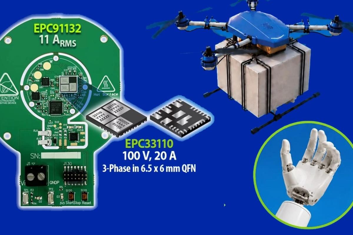
EPC Adds Compact 3-Phase BLDC Motor Drive Inverter
EPC has launched the EPC91132, a 23 mm 3‑phase BLDC motor‑drive inverter aimed at ultra‑compact applications such as humanoid wrist actuators and micro‑drones. The design integrates the EPC33110 GaN module, a 6 mm × 6.5 mm QFN chip that packs three half‑bridges, gate drivers and...
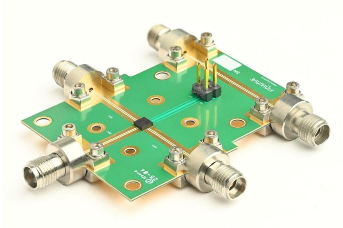
Finwave Highlights New Switch Range and X-Microwave Partnership
Finwave Semiconductor is debuting eight new GaN‑on‑Si RF switches at IMS2026 in Boston, showcasing high‑power, broadband performance in a 4 × 4 mm QFN package. The portfolio spans SPDT and SP4T designs, with power handling up to 40 W continuous‑wave and frequencies reaching 18 GHz,...

Onsemi Introduces GaNEXUS GaN Portfolio
Onsemi has unveiled GaNEXUS, a new gallium‑nitride power portfolio spanning 40 V to 650 V. The family includes Smart FETs with built‑in protection and thermally enhanced packages that fit standard footprints. In low‑voltage AI server converters the devices shrink magnetics by up...

Semi Expands QSiC Module Range for SSTs and AC-DC
US‑based SemiQ has broadened its QSiC Dual3 half‑bridge MOSFET module family, introducing high‑thermal‑performance versions that use aluminum‑nitride substrates and pre‑applied thermal interface material, as well as new 1700 V devices with as low as 1.7 mΩ RDSon. The expanded lineup is aimed...
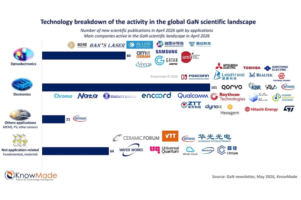
KnowMade Details a Rapidly Evolving Role for GaN
KnowMade’s monthly GaN update reports a surge in research and patent activity, with 327 new scientific papers and 362 new patent publications worldwide. Electronics applications lead the field, accounting for 162 papers and 238 patents, while optoelectronics remains vibrant with...

CGD's 650V ICeGaN Devices Improve EV Range
Cambridge GaN Devices (CGD) unveiled a 650 V ICeGaN power‑IC for automotive inverters, featuring a low 9 mΩ on‑resistance and integrated temperature sensing. The device simplifies parallel operation of multiple GaN chips, eliminating the need for matched performance or extra balancing components....
Fraunhofer IAF to Show GaN4EmoBil Module at PCIM
Fraunhofer Institute for Applied Solid State Physics IAF will showcase a GaN‑based power module for 800 V bidirectional DC charging at the PCIM Expo in Nuremberg (June 9‑11, 2026). The module, part of the BMWE‑funded GaN4EmoBiL project, uses 1200 V GaN devices on...
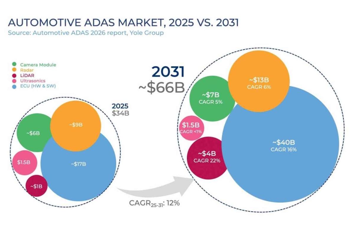
ADAS Focus Shifts From Sensors to Software
Yole Group’s Automotive ADAS 2026 report says the industry is moving from a sensor‑centric model to software‑defined platforms. Sensor demand stays robust, but the fastest growth now comes from centralized computing and software integration. The market is projected to exceed...

Silanna Far-UVC LEDs Counter H5N1 Bird Flu
University of Siena researchers demonstrated that 235 nm far‑UVC LEDs can inactivate the H5N1 avian influenza virus by up to 99.999% within seconds. The findings were unveiled at MEDICA 2025 in Düsseldorf, highlighting a biologically safe alternative to traditional 254 nm mercury lamps....

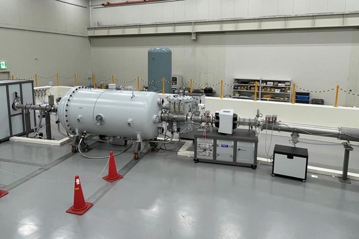
SiC Substrates with Table-Top Closed-Space PVT
Researchers at the University of Erlangen‑Nürnberg have unveiled a compact, table‑top close‑space physical vapour transport (CS‑PVT) system for silicon‑carbide (SiC) crystal growth. The tool operates at roughly 1900 °C under ultra‑high vacuum, delivering radial thermal gradients an order of magnitude lower...
Strengthening the World's First CS Cluster
The UK’s Strength in Places Fund (SIPF) has poured £43 million (≈$55 M) into South Wales, turning an existing concentration of compound‑semiconductor firms, universities and government into a coordinated ecosystem. Key technical milestones include IQE’s scale‑up of InP epitaxy to 6‑inch wafers...
SiC: Enhancing Reliability with Ion Implantation
Silicon‑carbide (SiC) power devices are rapidly gaining market share, but bipolar degradation caused by basal‑plane dislocations still limits yield and drives up costs. Researchers from Nagoya Institute of Technology, Nagoya University and ion‑implantation specialist Shi‑Atex demonstrated that high‑energy ion implantation—using...

EC Approves €66m for German SiC Facility
The European Commission has approved a €288 million (≈$314 million) state‑aid package for two German semiconductor projects. €66 million (≈$72 million) will fund Zadient Materials Europe’s new plant in Bitterfeld to produce high‑purity silicon‑carbide (SiC) source material using a circular gas‑recovery process. The remaining...
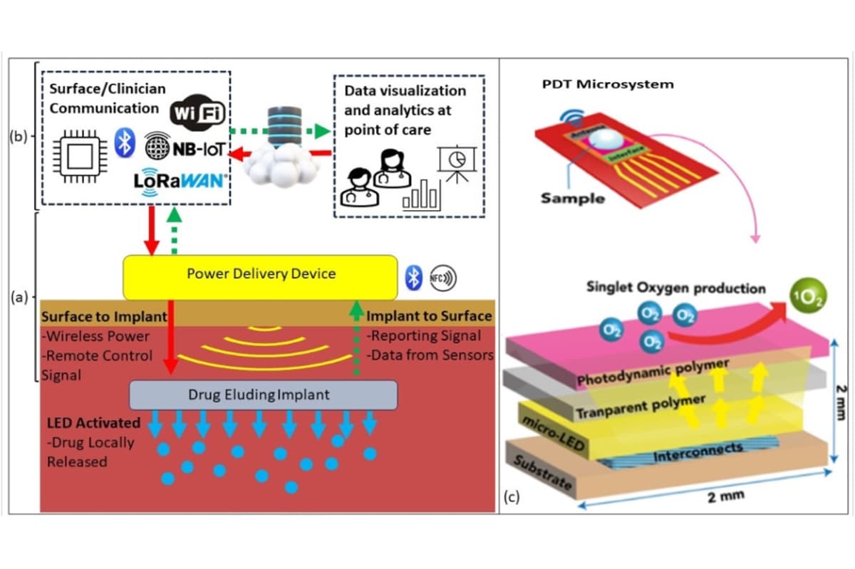
MicroLED Implant Could Cast New Light on Cancer Treatment
Engineers and cancer scientists at the University of Glasgow have created a flexible, disc‑shaped implant that houses wirelessly powered microLEDs to enhance photodynamic therapy for bladder cancer. The 40 mm device can deliver optical power exceeding five milliwatts and penetrate synthetic...