
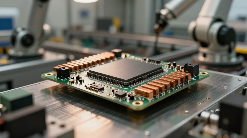
ACM Research Unifies Product Portfolio as ACM Planetary Family
ACM Research announced the ACM Planetary Family, a unified branding that reorganizes its equipment into eight process‑aligned series covering cleaning, advanced packaging, electroplating, furnace, track, PECVD, panel‑level packaging, and polishing. The new structure reflects the company’s evolution from a single cleaning tool in 1998 to a comprehensive portfolio serving front‑end, advanced packaging, and panel‑level markets. By aligning products with key semiconductor manufacturing steps, ACM aims to streamline customer selection and reinforce its technology differentiation strategy. CEO Dr. David Wang highlighted the move as a foundation for platformization and global customer outreach.
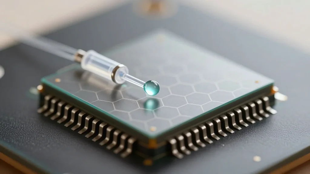
IVWorks Raises $4.5m to Expand reGaN Technology Into RF and AI Power Semi Markets
IVWorks Co Ltd, a South Korean GaN wafer maker, secured $4.5 million in new funding, raising its total investment to $33 million. The capital will expand its proprietary reGaN selective‑area regrowth technology into E‑band and W‑band RF markets and AI‑focused power‑delivery applications....

IIT-M Pravartak, Maven Silicon Launch Semiconductor Certification Programmes
IIT‑M Pravartak Technologies Foundation has teamed up with Maven Silicon to roll out two nine‑month semiconductor certification programmes covering VLSI design and verification as well as embedded systems design. The curriculum blends online instruction, hands‑on laboratory work, and industry‑focused capstone...

The Specialty Device Surge Part 2: The Process Control Challenges Of MEMS, Co-Packaged Optics, And More
The second installment of the Specialty Device Surge series highlights how MEMS, CMOS image sensors, SiC/GaN power devices, and co‑packaged optics are confronting unprecedented process‑control hurdles as wafer sizes expand to 300 mm. Each device family relies on unique materials—piezo films,...

Enhancing Silicon Reliability With In-System Test And SLM Data
The semiconductor industry is leveraging in‑system test (IST) and Silicon Lifecycle Management (SLM) data to boost chip reliability across design, manufacturing, and field operation. Traditional DFT methods such as ATPG, scan chains, and BIST remain core, but embedded monitors and...
Kandou AI Raises $225M in Series A Funding
Swiss fabless startup Kandou AI secured a $225 million Series A round led by Maverick Silicon, with SoftBank, Synopsys, Cadence and Alchip participating. The funding will accelerate production of its Copper MIMO (chord signaling) chips that aim to double data‑rate capacity while slashing...
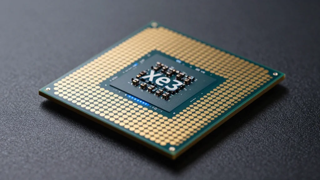
Intel Nova Lake to Use Xe3 Graphics, AX High-End Variant Cancelled
Intel’s upcoming Core Ultra 400 "Nova Lake" CPUs will ship with existing Xe3 graphics rather than the anticipated Xe4 architecture, while higher‑tier models will receive an enhanced Xe3P variant. The company also cancelled the high‑end AX SKU for this generation,...
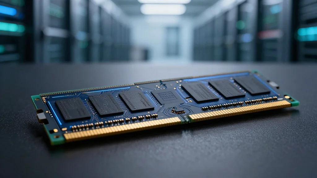
Samsung Sees Massive 600 Percent Q1 Profit Surge as DRAM Market Tightens
Samsung Electronics is projected to post a record Q1 2026 operating profit of about $23.7 billion, a 600% year‑over‑year increase driven by a tightening DRAM market. The semiconductor division’s gross margin surged to roughly 80%, up from 15% a year earlier, as...
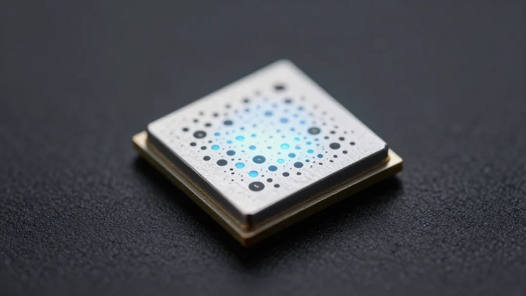
Archer Materials Advances Silicon Biochip Beta Prototype While Reaffirming Graphene as Next‑generation Platform
Archer Materials announced that its Stage 1 biochip project with IMEC is complete and the company is moving to a silicon‑based beta prototype. The prototype will combine a functionalized potassium sensor with cartridge engineering, microfluidics, and readout electronics for external validation....
Renesas Rad-Hard ICs Aboard NASA’s Artemis II
Renesas Electronics’ radiation‑hardened integrated circuits are aboard NASA’s Artemis II mission, which launched on April 1 from Kennedy Space Center. The Intersil‑branded rad‑hard ICs are embedded in Orion’s avionics and the Space Launch System, managing power distribution, signal integrity and onboard computing...
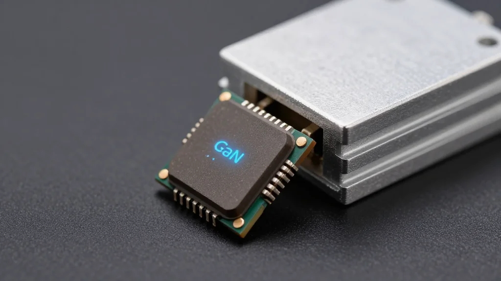
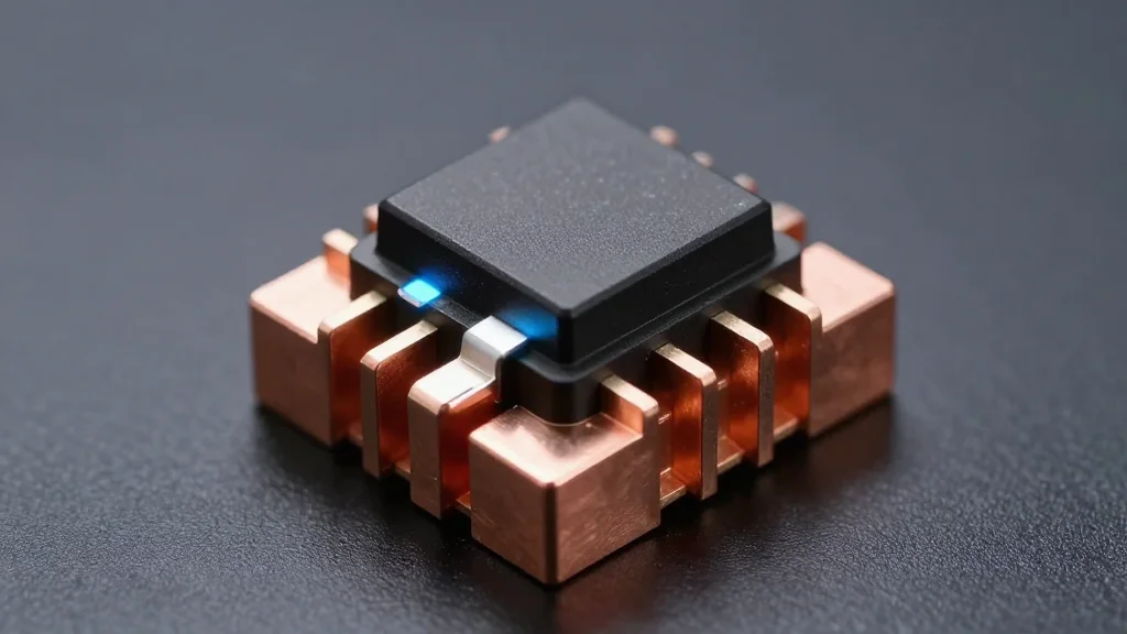
EPC Expands Portfolio of 100V Integrated GaN Power Stage ICs
Efficient Power Conversion (EPC) has launched a 100 V GaN power‑stage IC family—EPC23108, 23109, 23110 and 23111—targeted at high‑performance motion and power‑dense platforms such as humanoid robots and drones. Each device integrates high‑side and low‑side eGaN FETs, gate drivers and level‑shifting...
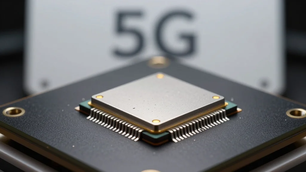
Sivers Announces 5G/6G ICs
Sivers Semiconductors has launched the Daybreak 7‑15 GHz beamforming ICs, now generally available for emerging 5G‑Advanced and 6G FR3 applications and defense arrays. The chips deliver industry‑leading broadband transmit power, high efficiency and a low receiver noise figure, while supporting external...
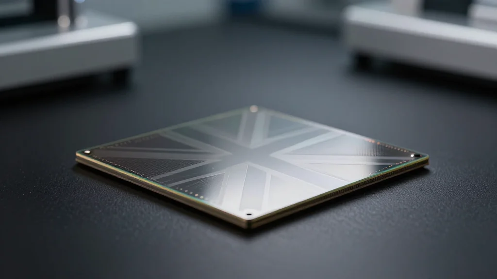
£10.4m UK Project Will Grow Next-Gen Materials
The UK’s Engineering and Physical Sciences Research Council has awarded £10.4 million to a five‑year EXPRESS programme led by the Universities of Warwick and Southampton. The project will develop electrochemical electrodeposition techniques, guided by bespoke precursor chemistry, to grow high‑quality transition...
Silvaco Announces SiC Partnership with APEC
Silvaco Group announced an expanded strategic partnership with Taiwan‑based Advanced Power Electronics Corp. (APEC) to deepen the use of its Victory Device, Gateway, and SmartSpice solutions. APEC will deploy these tools across its silicon and silicon‑carbide (SiC) product lines, aiming...
Onsemi Powers Sineng's Solar and Energy Storage Systems
Onsemi’s latest hybrid power integrated modules, combining FS7 IGBTs with EliteSiC diodes in an F5BP package, have been selected for Sineng Electric’s next‑generation 430 kW liquid‑cooled string energy storage system and its 320 kW utility‑scale solar inverter. The modules deliver up to...
EPC Space Adds Half-Bridge Buck Platforms
EPC Space introduced two new eGaN half‑bridge buck evaluation boards, the EPC7C010 and EPC7C011, targeting aerospace and industrial power applications. The EPC7C010 delivers 100 V/20 A at up to 94.7% efficiency, while the EPC7C011 offers 200 V/10 A with a peak 96.6% efficiency. Both...
UK Semiconductor Centre Appoints Two New Directors
The UK Semiconductor Centre (UKSC) has hired Martin O’Sullivan as Director of Investment and Steve Taylor as Director of Strategic Marketing. O’Sullivan, a PhD‑trained semiconductor physicist with a background in equity research and capital markets, will streamline investor relations and...
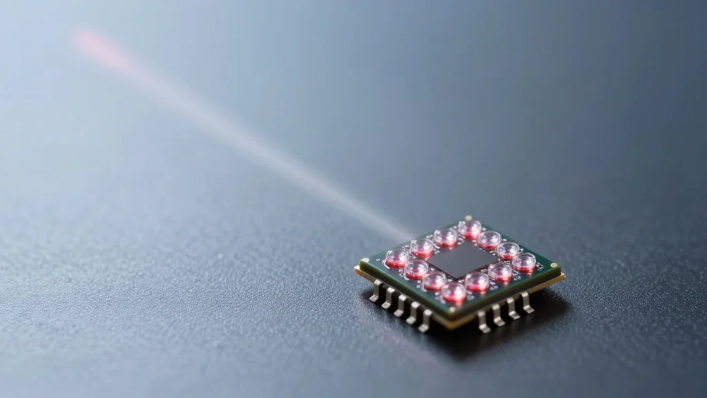
Tiny Laser Array Could Offer Faster, Greener Indoor Wireless
British researchers have built a sub‑millimetre chip that integrates a 5 × 5 infrared VCSEL array with custom beam‑shaping optics, creating a compact optical wireless transmitter. Individual lasers deliver 13‑19 Gbps, and together they achieve a record‑breaking 362.7 Gbps over a two‑metre free‑space link....
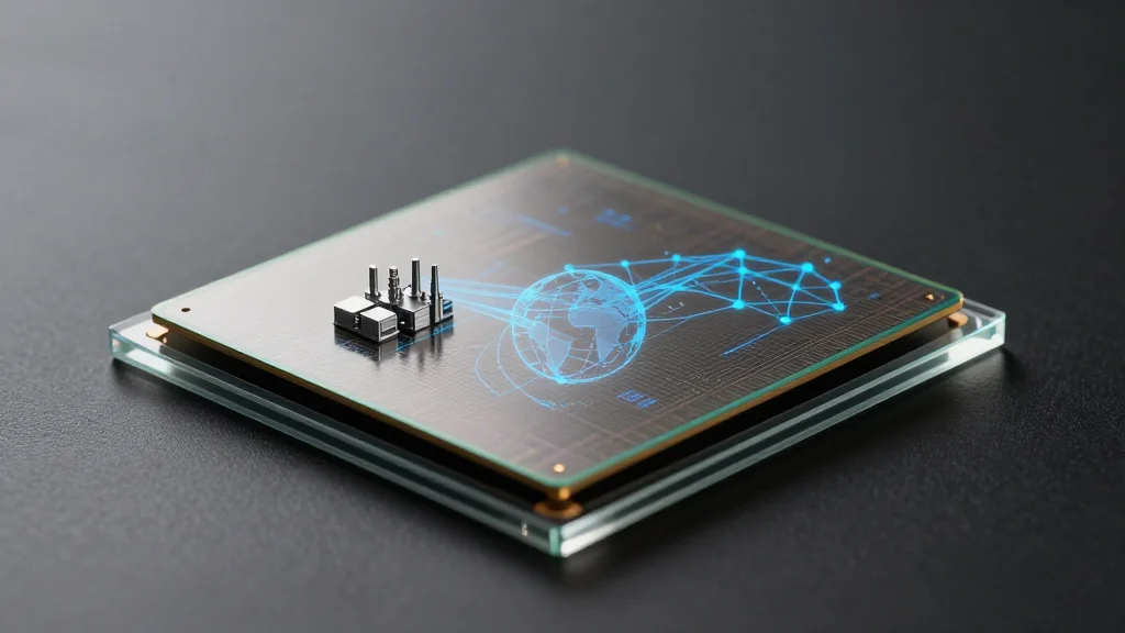
Digital Twin Semiconductor Supply Chain Market to Reach $7.9 Billion by 2033
The Digital Twin Semiconductor Supply Chain market is forecast to reach $7.9 billion by 2033. Growing demand for end‑to‑end visibility, faster time‑to‑market and resilient operations is driving adoption across the industry. Digital twins provide real‑time simulation, predictive analytics and process automation,...
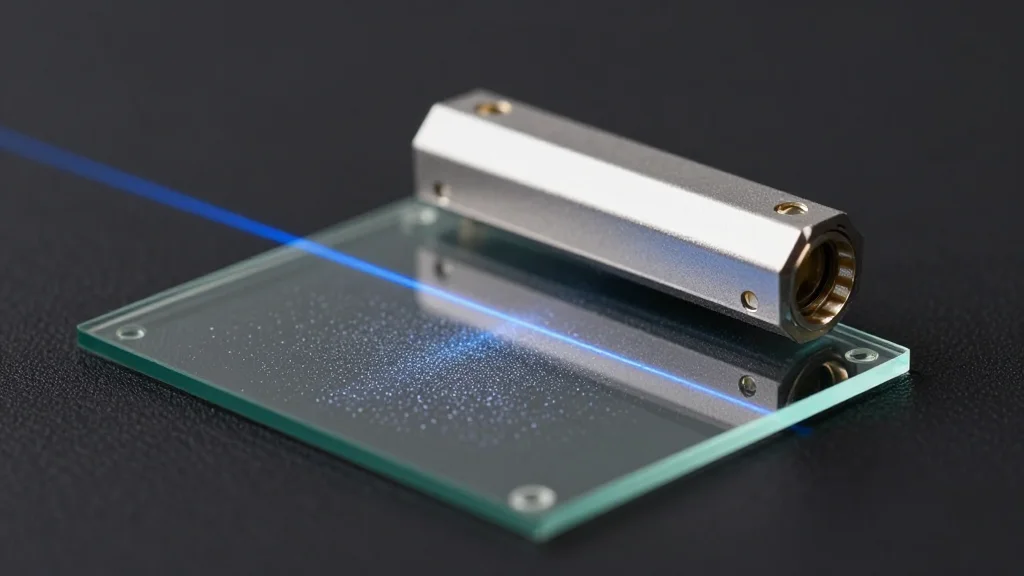
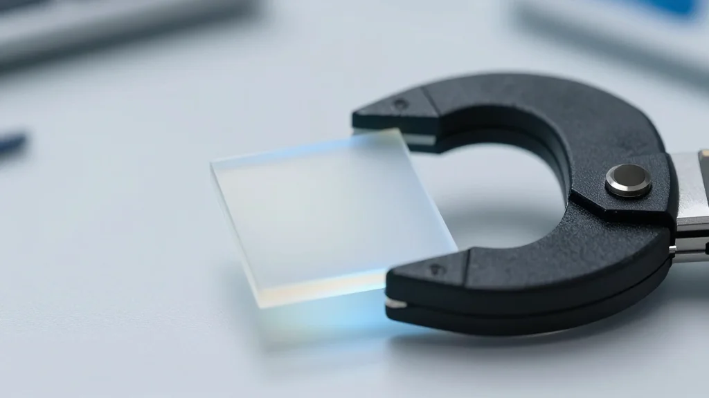
SmartRay Sensor Unites ECCO X Innovations with High-Precision Glass Inspection Capabilities
SmartRay unveiled the ECCO X 050G sensor, extending its ECCO X family with high‑resolution inline metrology for glass, reflective and transparent surfaces. The sensor delivers up to 40 kHz scan rates, 2.2–2.9 µm vertical and 11–13 µm lateral resolution, and generates 163 million 3‑D points per second...

Quantum Diamonds Expands to Asia
QuantumDiamonds announced the launch of a new regional hub in Taiwan, marking its first major foothold in Asia. The company appointed Peter Lemmens, a veteran with over 25 years in semiconductor leadership, to spearhead commercial and technical operations across the...
CEA-Leti and Fraunhofer IPMS Validate Wafer Exchange for Ferroelectric Memory Materials
CEA‑Leti and Fraunhofer IPMS have successfully demonstrated a wafer‑exchange pilot line for hafnium‑zirconium‑oxide ferroelectric stacks, proving that complex material stacks can be processed across multiple advanced fabs without contamination. The program used 300 mm CMOS cleanrooms, standardized VPD‑ICP‑MS and TXRF checks,...
Imec Names NVIDIA's Jensen Huang as Recipient of the 2026 Imec Lifetime of Innovation Award
Imec announced that Jensen Huang, founder and CEO of NVIDIA, will receive the 2026 imec Lifetime of Innovation Award. The award honors Huang’s pivotal role in creating the programmable GPU, which has evolved from gaming graphics to the core engine...
Keysight Introduces Hands-On Semiconductor Teaching Labs for Universities
Keysight Technologies unveiled three semiconductor teaching lab solutions—Basic Design and Measurement, Parametric Test and On‑Wafer Measurement, and Photonics IC Measurement—to give university students hands‑on experience with professional‑grade tools. The kits replicate real‑world test workflows, letting students set up equipment, perform...
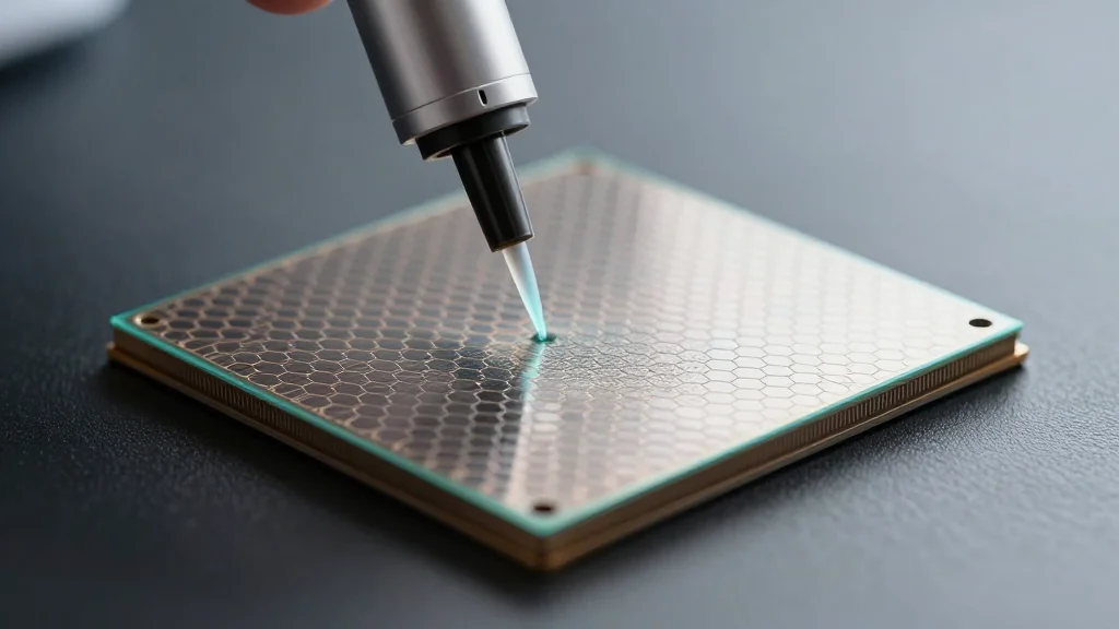
Nordson Electronics Solutions to Demonstrate Automated Fluid Dispensing and Plasma Treatment Systems
Nordson Electronics Solutions will demonstrate its ASYMTEK Vantage fluid dispensing system with a new Class‑100 cleanroom configuration at Productronica China. The company will also showcase the stand‑alone MARCH FlexTRAK plasma system, which provides high‑throughput surface treatment in a compact footprint....
Metallic Oxide Semiconductor Field Effect Transistor Market to Surpass $15.5 Billion by 2033
The global metallic oxide semiconductor field‑effect transistor (MOSFET) market is projected to exceed $15.5 billion by 2033, driven by surging demand for energy‑efficient consumer electronics, electric vehicles, and renewable‑energy systems. Wide‑bandgap silicon‑carbide and gallium‑nitride technologies are accelerating performance gains, while miniaturization...
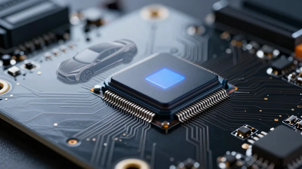
Automotive Semiconductor Shifts & AI Workloads | TechInsights AWS Seminar
TechInsights hosted a data‑driven seminar for AWS automotive teams, highlighting a decisive shift from distributed electronic modules to centralized compute architectures in vehicles. The briefing detailed how high‑performance automotive SoCs, expanding memory bandwidth, and silicon‑carbide power devices are reshaping AI...

Hong Kong: Secure Edge AI with Compute-in-Memory Innovation
University of Hong Kong researchers unveiled a Co‑Located Authentication and Processing system that merges compute‑in‑memory with hardware‑based security using memristors. The architecture eliminates the von Neumann bottleneck, delivering a 146‑fold boost in energy efficiency and an 18‑fold reduction in chip area...

European Chips Skills Academy Launches the ECSA Learning Platform
The European Chips Skills Academy (ECSA) has launched the ECSA Learning Platform, a free digital hub offering more than 60 introductory to intermediate semiconductor courses. Developed with industry and academic partners, the platform integrates a Knowledge Hub, community collaboration spaces,...
Semiconductor-Based Quantum Pilot Line ‘SPINS’ Launched with EU Support
The EU has launched the €50 million SPINS pilot line, one of six quantum pilot facilities created under the Chips Act. Coordinated by imec, SPINS unites 25 RTOs, industry players and universities to develop semiconductor‑based spin‑qubit chips. The initiative targets three...
Stitching Precise Patterns – With Lasers
University of Pittsburgh engineers have devised a laser‑induced graphene (LIG) manufacturing method that uses an iron‑oxide ink layer to precisely control graphene formation on polymer films. The technique enables tunable electrode thickness and conductivity, and can create graphene on either...
IVWorks Secures $4.5M Funding to Expand ‘reGaN’ Technology Into RF and AI Power Semiconductor Markets
IVWorks announced a $4.5 million financing round, bringing its total capital raised to $33 million, to accelerate deployment of its proprietary reGaN technology. The company will use the funds to scale mass‑production infrastructure and secure its supply chain for GaN epitaxial wafers...
US Lawmakers Aim to Ban Export of DUV Chipmaking and Etching Tools to Leading Firms in China — Bipartisan Proposal...
A bipartisan group of U.S. senators has introduced the MATCH Act, shifting export controls on advanced wafer‑fabrication equipment from fab‑level to company‑level restrictions. The bill would bar DUV lithography, etching and deposition tools from reaching Chinese firms such as Huawei,...

Why TSMC Grew Four Times Faster than Its Foundry Rivals in 2025 — Price Hikes, Vertical Integration, and Commanding Technology...
The semiconductor foundry market hit a record $320 billion in 2025, with TSMC commanding 38% and growing 36% YoY, far outpacing rivals that collectively rose 8%. Its dominance stems from an unprecedented volume of sub‑5 nm wafers, aggressive price hikes, and a...

IBM, Arm Target Enterprise AI With Mixed-Architecture Approach
IBM and Arm announced a partnership to run Arm‑native applications on IBM Z mainframes and LinuxOne servers through a shared software layer and virtualization. The solution lets enterprises deploy AI workloads across both architectures without rewriting code, preserving the uptime,...

ACCM Celeritas™ SF1600 Delivers Zero-Skew for PCIe 7, 224 Gbps and Beyond
Advanced Chip & Circuit Materials (ACCM) launched Celeritas SF1600, a laminate and prepreg that eliminates fiber‑weave skew, a root cause of timing errors in 224 Gbps PAM4 and higher data rates. The material delivers zero‑skew performance, a low dielectric constant of 2.80,...
CEA-Leti, CEA-List and PSMC Collaborate to Integrate RISC-V and MicroLED Silicon Photonics Into 3D Stacking and Interposer for...
CEA‑Leti, CEA‑List and Powerchip Semiconductor Manufacturing Corporation (PSMC) announced a partnership to embed CEA‑List’s RISC‑V processor IP and CEA‑Leti’s microLED silicon‑photonic chiplets into PSMC’s 3D‑stacking and interposer platform. The integration replaces traditional copper interconnects with short‑reach, high‑bandwidth optical links, delivering...
Vishay Launches Automotive PV MOSFET Driver
Vishay Intertechnology has released the VODA1275, an automotive‑grade photovoltaic MOSFET driver built in a compact SMD‑4 package with an 8 mm creepage distance and a CTI‑600 mold compound. The driver offers 20 V open‑circuit voltage, 20 µA short‑circuit current, and an 80 µs turn‑on...

DigiKey Collaborates with STMicroelectronics and Ultra Librarian on eDesignSuite
DigiKey, STMicroelectronics, and Ultra Librarian have launched an enhanced eDesignSuite, a free browser‑based design platform that unifies simulation, component selection, and BOM purchasing. The tool supports power‑management, signal‑conditioning, and NFC/RFID applications, offering multi‑CAD export and direct integration with DigiKey’s catalog....

Parsing the AI and Gaming Future with Nvidia’s Jensen Huang | GTC Q&A
Nvidia CEO Jensen Huang delivered an unscripted two‑hour keynote at GTC 2026, unveiling more than a dozen AI‑focused gaming announcements. The event in San Jose attracted over 30,000 attendees, underscoring the growing appetite for AI‑driven technology in entertainment. Huang highlighted...
Silicon Choices Grow in Importance as Industrial AI Moves Closer to the Factory Floor
Industrial AI is moving from centralized clouds to the factory floor, where real‑time inference must run continuously alongside machines. This shift is driven by latency, data volume, and security concerns that make edge processing essential. As a result, the choice...
EPC’s CEO Analyzes GaN’s Move Into Robotics and Data Centers
Over the past few years GaN HEMTs have moved beyond consumer chargers into high‑performance markets such as AI data‑center servers and humanoid robotics. EPC’s CEO Alex Lidow explained that the material’s low on‑resistance, ultra‑fast switching and high power density make it...
Indium Corporation Announces Strategic Agreement for Domestic Critical Metals Recovery
Indium Corporation has signed a long‑term offtake framework with Flash Metals USA, a Metallium subsidiary, to purchase critical metals recovered from electronic scrap using Flash Joule Heating technology. The agreement covers gallium, germanium, copper, tin, gold and indium, with an...
Japan's Rapidus Ramps up 2nm Chip Plans While Eyeing Factories on the Moon
Japan’s state‑backed chipmaker Rapidus has moved its IIM‑1 plant in Hokkaido from construction to an operating pilot line, delivering working two‑nanometer gate‑all‑around prototypes. The company secured a ¥267.6 billion ($1.7 billion) financing round led by the government and over 30 private partners,...

Supermicro Owes Its Rapid Rise to $4 Trillion Nvidia—But China Smuggling Allegations and a High-Profile Arrest Could Blow up the...
Supermicro’s rapid growth has been powered by its deep reliance on Nvidia GPUs, which now account for roughly 64% of its component spend and drive about 71% of its revenue. A federal indictment alleges co‑founder Yih‑Shyan “Wally” Liaw smuggled $2.5 billion...
Research Bits: Apr. 6
Researchers at Loughborough University unveiled a nanoporous niobium‑oxide memristor that performs reservoir computing directly in hardware, achieving up to 2,000‑times lower energy consumption than conventional software solutions. The same chip accurately forecasted short‑term Lorenz‑63 chaos, recognized pixelated digits and executed...
NXP Introduces Omlox Starter Kit for Industrial RTLS Deployment
NXP Semiconductors has launched the omlox Starter Kit, a turnkey solution that merges UWB hardware, software and analytics into a single platform built on the omlox open standard. The kit centers on NXP’s Trimension SR048 UWB SoC and MCX W72...

Global 300mm Fab Equipment Spending Set to Rise, AI Drives Semiconductor Investment
Global spending on 300 mm wafer fab equipment is projected to reach $133 billion in 2026, an 18 % rise. The upward trajectory continues to $151 billion in 2027, driven by surging AI chip demand in data centers and edge devices. Logic and micro‑devices...

Murata Completes New MLCC Production Facility in Izumo, Japan
Murata Manufacturing has finished a new 10‑story, 69,829 m² multilayer ceramic capacitor (MLCC) plant in Izumo, Japan, after two years of construction. The project cost about 47 billion yen (≈ $313 million) and expands Murata’s production footprint in the region. The facility complements Murata’s...

TSMC Plans GigaFab Cluster in Arizona, Aiming for Capacity Close to Taiwan
Taiwan Semiconductor Manufacturing Co. (TSMC) is accelerating its U.S. footprint by planning a GigaFab cluster in Arizona that would rival the output of its Hsinchu facilities in Taiwan. The project is part of a broader rollout of 12 plants across...