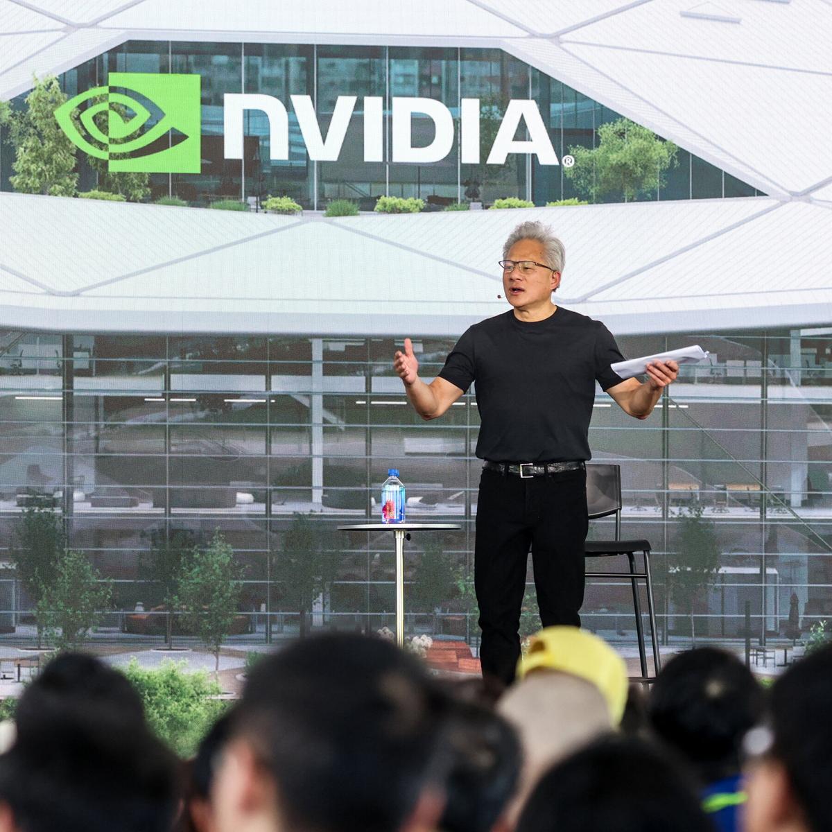
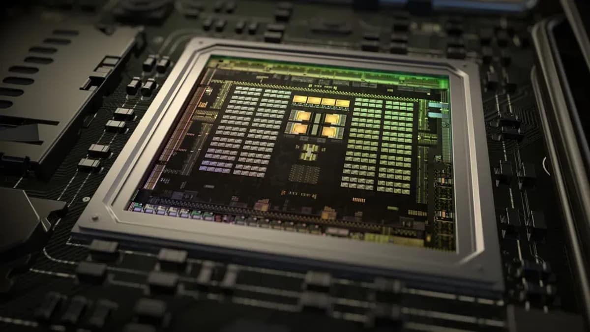
NVIDIA Names Anthropic and OpenAI Among First Users of Its Vera Chip
Nvidia announced that Anthropic, OpenAI, SpaceX and Oracle are among the first customers of its new Vera data‑center CPU, the successor to Grace. Vera replaces off‑the‑shelf Arm cores with 88 in‑house Olympus cores and offers up to 1.2 TB/s memory bandwidth, positioning itself for AI‑agent workloads. Independent benchmarks show Vera out‑performing Intel Xeon and AMD EPYC on several metrics. Oracle Cloud will be the first hyperscaler to run Vera at scale, with broader cloud availability slated for the second half of 2026.

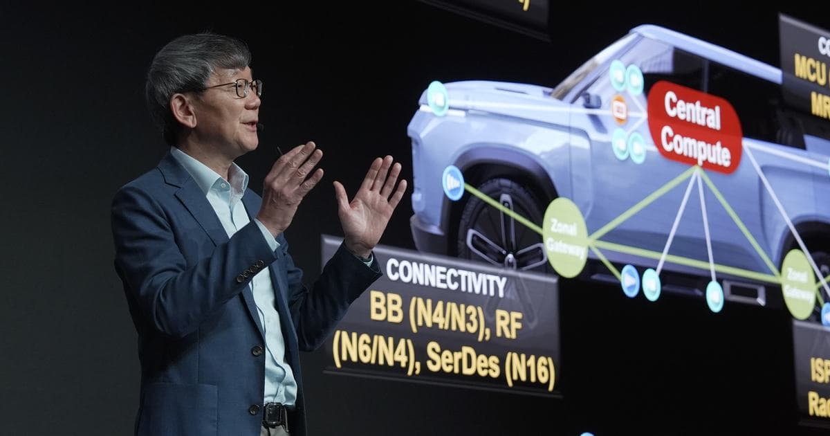
MICROIP Debuts AI Vehicle System Business Group at COMPUTEX 2026
MICROIP announced the formation of an AI Vehicle System Business Group at Computex 2026, showcasing edge‑AI hardware and software aimed at automotive safety and fleet management. The group unveiled dual AI platforms—AIVO, a no‑code vision builder, and XEdgAI, a hardware‑agnostic...
Nvidia Has a Plan to Put Its Chips in Personal Computers
Nvidia announced its RTX Spark processor, a GPU‑accelerated chip designed to run local AI agents on Windows laptops and desktops. The company has secured partnerships with Dell, HP, Lenovo, Microsoft and other OEMs for a fall 2026 launch. RTX Spark promises on‑device...

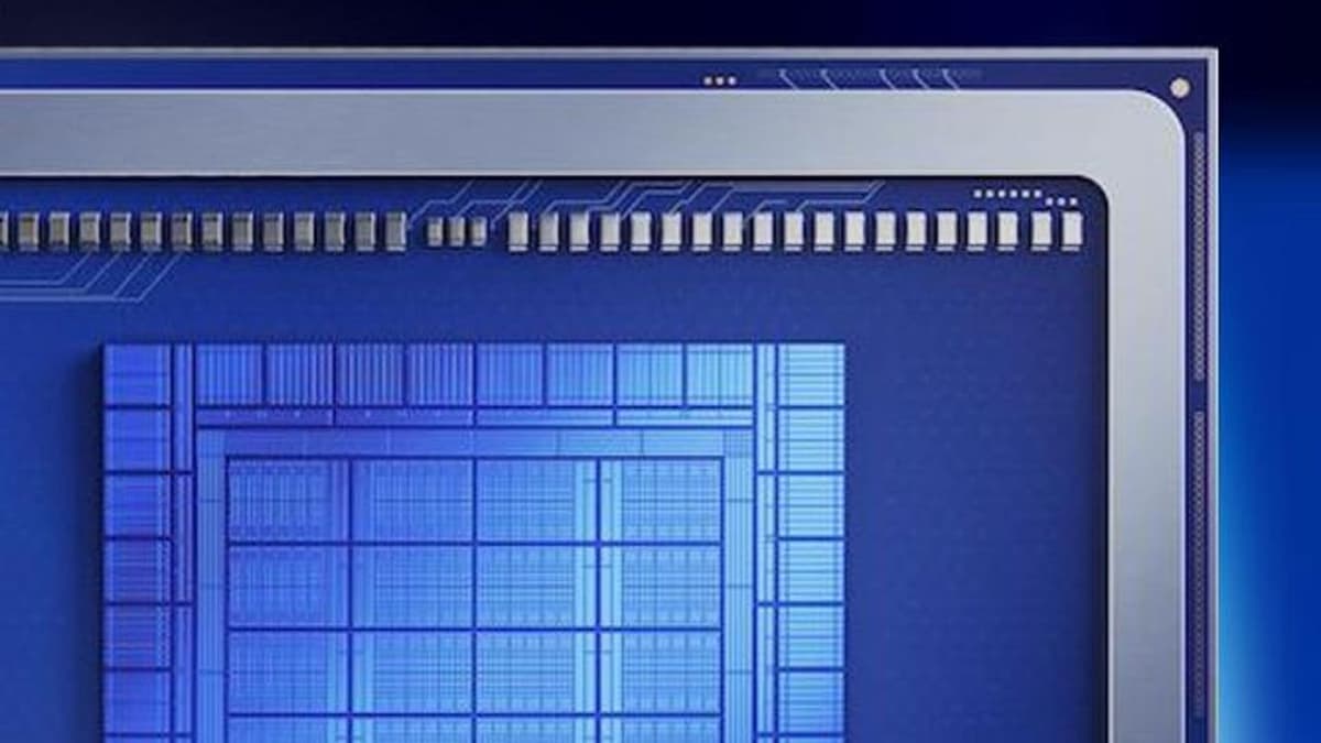
The Sub-2nm Paradox
The semiconductor industry is confronting a paradox at sub‑2nm nodes: while transistor density continues to rise, process variation, RC delay, and SRAM scaling limits are driving yields down and costs up. Foundries are extending node roadmaps to 10 angstrom (≈1 nm) and...
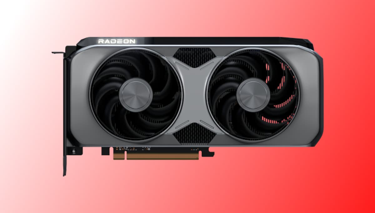
AMD Launch the Radeon RX 9070 GRE, Ryzen 7 7700X3D, Expanded Socket AM5 Support and More
At Computex 2026 AMD announced a multi‑year commitment to its AM5 platform through 2029 and unveiled the Ryzen 7 7700X3D, a new 3D V‑Cache processor priced at $329 and shipping July 16. The company also launched the Radeon RX 9070 GRE, a mid‑range RDNA 4 GPU aimed at...

AMD Extends AM5 Socket Support Through 2029 for Future Ryzen CPUs
AMD announced at Computex that its AM5 socket will remain supported through 2029, extending the previous 2027 guarantee. The roadmap now covers current Zen 5 Ryzen 9000 chips and upcoming Zen 6 processors, with hints that Zen 7 may also use the socket. By...

NVIDIA Commits to New Windows Arm Processors Every Two Years
NVIDIA announced a long‑term Windows processor roadmap, pledging new Arm‑based CPU platforms every two years through 2030. The first products, under the RTX Spark brand, will launch later this year in notebooks before expanding to mini‑PCs and desktops. A high‑end...

If Cores Are What Agents Crave, Intel's New Clearwater Xeon 6+ Might Just Quench Their Thirst
Intel unveiled the Clearwater Forest Xeon 6+ processor, delivering up to 288 cores per socket to target agentic AI workloads that rely heavily on CPU threads. The chip uses a 2 nm‑class process, stacking twelve 24‑core tiles with I/O dies borrowed...

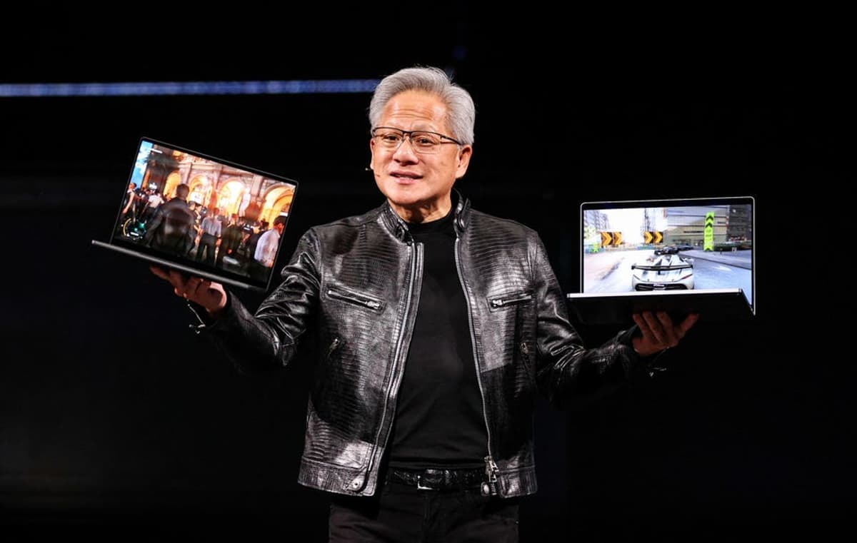
Nvidia Jumps Into PCs with New Arm-Based Chip Debuting in Laptops From Microsoft, Dell, HP
Nvidia unveiled its first ARM‑based PC processor, the N1X, integrated into the RTX Spark superchip. The new chip will appear in laptops from Microsoft, Dell, HP, ASUS, Lenovo and MSI, with more than 30 laptops and 10 desktops slated for release....
Nvidia Shows Off First Windows Laptops And Desktops Powered Entirely By Its Own Chip
Nvidia unveiled the RTX Spark chip, a consumer‑grade processor that combines the company’s AI‑focused GPU with a custom‑built CPU. The chip is designed to run local “personal AI agents” while handling high‑end gaming and productivity workloads such as Adobe Photoshop. Nvidia...

ASML Spinout Invisix Raises €20M to See Inside the Chips Optics Can’t
Invisix, an ASML spin‑out from Eindhoven, closed an oversubscribed seed round, raising €20 million (about $22 million). Investors include Hitachi Ventures, imec.xpand, Doosan Investment and a tier‑1 semiconductor manufacturer, likely Samsung. The startup will use the capital to build a soft‑x‑ray metrology...
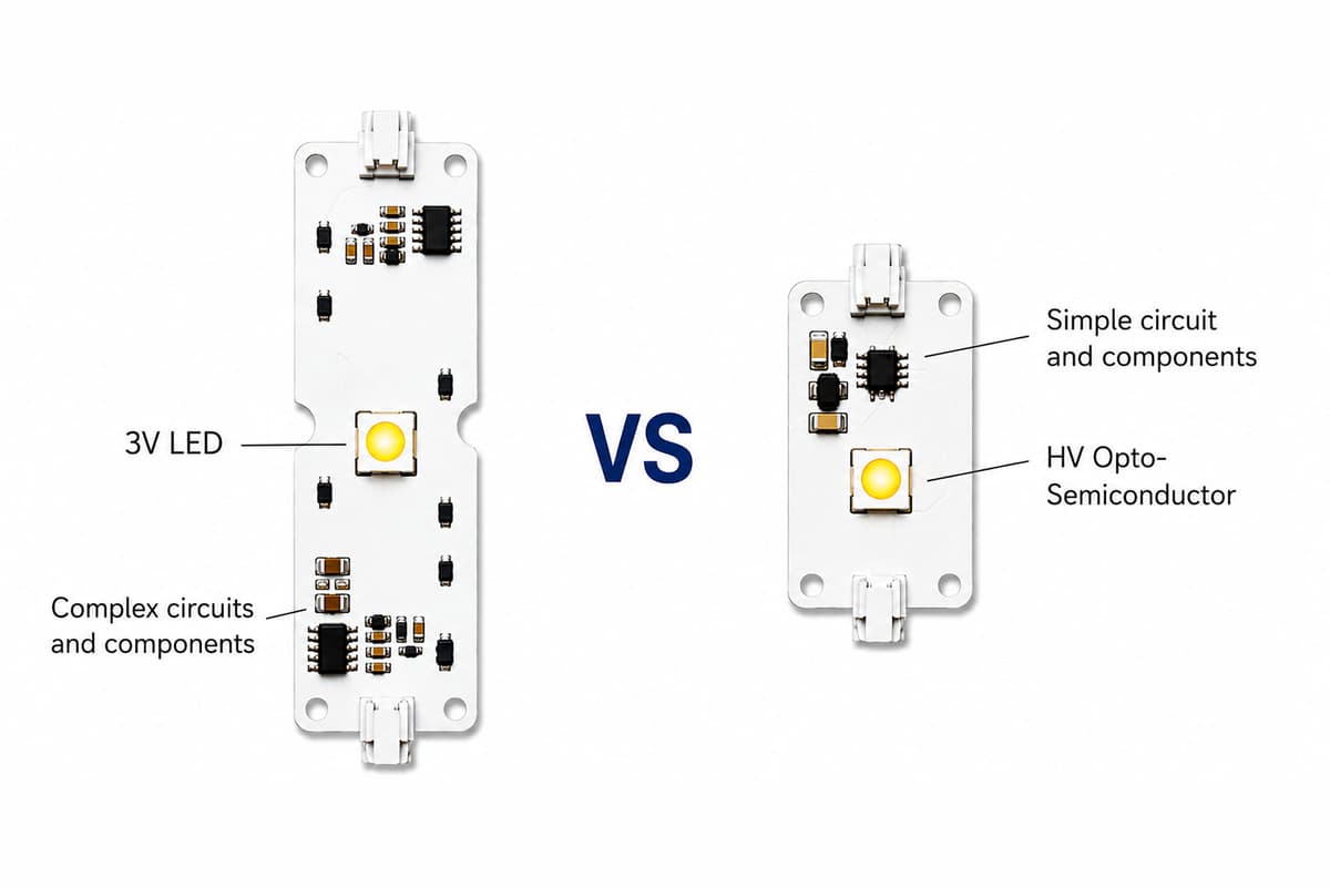
Seoul Semiconductor Launches HV Opto-Semiconductor for EVs
Seoul Semiconductor has begun mass‑producing its high‑voltage (HV) opto‑semiconductor chips with four major automakers across the Americas, Europe and Asia. The new devices run on a 12 V single‑chip architecture, replacing conventional 3 V LED setups and trimming driver component counts by...
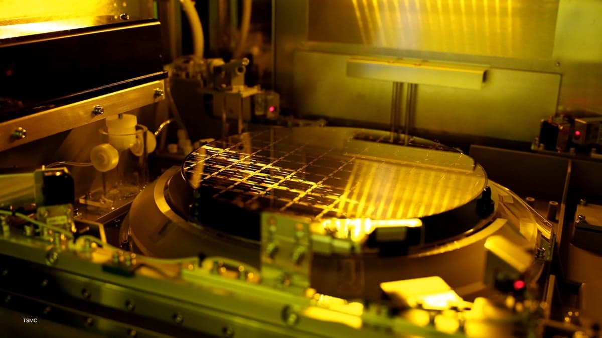
TSMC Uses Nvidia AI to Advance Semiconductor Design and Manufactuing
TSMC announced it is integrating Nvidia’s accelerated computing and AI tools across its semiconductor design and manufacturing workflow. The partnership leverages Nvidia CUDA‑X libraries, cuLitho, cuEST, cuML, H200 GPUs, Metropolis, TAO Toolkit, and Omniverse to cut lithography cycle time by...
Nvidia Unveils PC ‘Superchip’ in Challenge to Apple and Intel
Nvidia announced a new PC‑focused "superchip" that fuses an Ada‑generation GPU with a custom ARM‑based CPU, creating a single package for high‑performance laptops and desktops. The chip promises up to twice the AI inference speed of current RTX 40‑series GPUs...
Intel Focuses on Power Efficiency and Cost with New Chip Designs
Intel unveiled three data‑center products—Xeon 6+ CPU, Crescent Island GPU, and the E835 Ethernet card—designed to curb power draw and lower total‑cost of ownership for AI workloads. The GPU, built for agentic AI, uses 480 GB of LPDDR5X memory and runs at...
Intel Details Long-Awaited Crescent Island AI GPU at Computex, Boasts up to 480 GB of LPDDR5X to Combat Memory Shortages...
Intel unveiled details of its upcoming Crescent Island GPU at Computex 2026, a PCIe add‑in card built on the Xe3P architecture aimed at agentic AI inference. The accelerator will forgo traditional GDDR or HBM in favor of up to 480 GB...
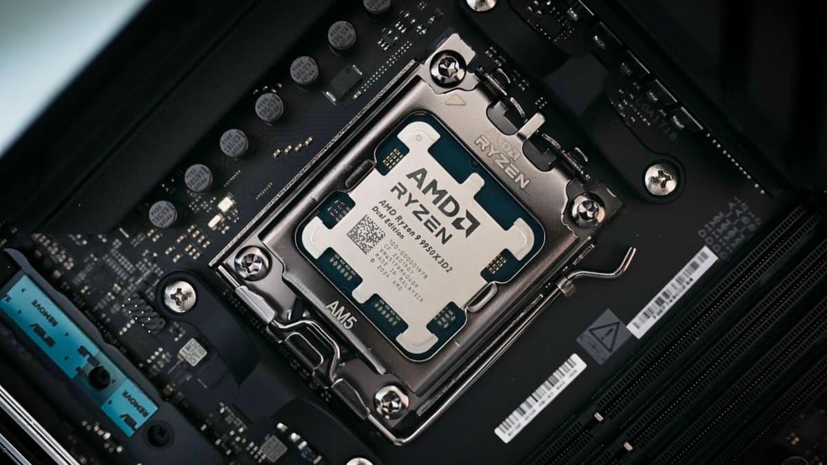
AMD Confirms AM5 Support Through 2029 — Zen 4 and 5 Platform Will Likely See Two More Generations, at Least
AMD announced at Computex 2026 that its AM5 socket will be supported through 2029, extending the original 2027 commitment. The extension implies at least two additional CPU generations, likely Zen 6 and Zen 7, will run on the same platform. AMD also previewed...
German Chipmaker Infineon to Expand India Ops with New R&D and Supply Chain Investments
Infineon Technologies, a German chipmaker among the world’s top ten, will nearly double its Indian workforce from 2,600 to about 5,000 by 2030. The expansion includes new R&D facilities and a strengthened supply‑chain network aimed at supporting India’s green‑energy transition....

ROHM Adds PLECS Simulator for Power Design Checks
ROHM has launched a free, browser‑based PLECS Simulator that lets power electronics engineers quickly calculate loss and temperature rise for its devices. The tool currently supports 20 topologies and will expand to include SiC, IGBT and module families. It is...
Marvell Technology: AI Growth Catalyst Is Kicking Off
Marvell Technology reported record Q1 revenue of $2.4 B, up 28% year‑over‑year, as custom AI chip demand and data‑center expansion accelerate. The company’s AI‑focused silicon business is becoming a critical supplier for hyperscale AI infrastructure, positioning it for continued growth. Analysts...

AMD to Invest $10 Billion+ in Taiwan
AMD announced a commitment of over $10 billion to expand its Taiwan ecosystem, targeting advanced packaging and AI‑focused silicon manufacturing. The funding will accelerate development of Elevated Fanout Bridge (EFB) interconnects and support the Helios rack‑scale AI platform slated for the...
X-FAB and Cadence Strengthen Collaboration
X‑FAB and Cadence have expanded their partnership to deliver a joint design‑migration solution that couples X‑FAB’s process‑specific PDKs with Cadence’s Virtuoso Studio automation tools. The offering enables customers to move designs from older CMOS nodes to newer geometries quickly, with a...
Nvidia and Microsoft Tease "a New Era of PC" Ahead of Computex 2026 — Coordinated Social Media Posts Could Indicate...
Nvidia and Microsoft are teasing the debut of the N1X AI laptop platform at Computex 2026, hinting it will run Windows on Arm. The device is expected to be powered by Nvidia’s GB10 Superchip, which combines an RTX 5070‑class GPU, a...
Why High-Bandwidth Memory Is a Bottleneck for AI Chips
AI's rapid expansion has exposed a memory bottleneck, putting high‑bandwidth memory (HBM) at the center of the hardware race. Micron Technology, the only U.S. memory‑chip maker, briefly hit a $1 trillion market valuation as its HBM4 chips promise more than 2.8 TB/s...

Accelerating 2nm & Advanced Packaging Through Global Collaboration
The article outlines how AI is reshaping semiconductor manufacturing, prompting Rapidus to pioneer an "AI Foundry" that couples 2nm process technology with advanced 3D packaging. By embedding sensors and machine‑learning analytics throughout the fab, Rapidus aims to slash design‑qualification cycles...
Energy Efficient Compute Is Most Important Attribute for Customers, TSMC Claims
TSMC says energy‑efficient compute has become the top priority for customers across edge, mobile, IoT, HPC and data‑center segments. The company is targeting a 30% efficiency gain per process generation and is on track despite plans for 1 MW‑plus chips by...
Intel and 3DGS Back a $3.3bn Glass-Substrate Plant in India’s Odisha
Intel and 3D Glass Solutions have signed an MoU to build a $3.3 billion glass‑core substrate plant in Odisha, India, over the next five to six years. The facility will target production of about 70,000 glass substrates, 50 million assembled units and...
Infineon Joins NVIDIA’s MGX AI Factory Ecosystem
Infineon Technologies has joined NVIDIA’s MGX AI Factory ecosystem, supplying 800 VDC power‑management solutions that integrate with NVIDIA’s modular MGX architecture. The partnership leverages Infineon’s silicon‑carbide (SiC) JFETs and gallium‑nitride (GaN) converters to deliver ultra‑compact, high‑efficiency bus conversion from grid to...

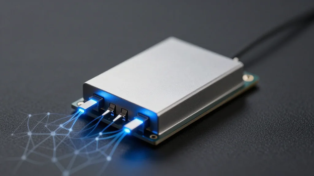
This Chip Startup Just Raised $135M on a Bet that AI’s Biggest Bottleneck Isn’t Compute — It’s Memory
XCENA, a South Korea‑U.S. chip startup, announced a $135 million Series B round that lifts its valuation to $570 million. The company’s MX1 processor embeds compute directly into DRAM using a CXL link, aiming to cut the costly data shuttling between CPUs, GPUs...
Real-Time LLM Inference on Standard GPUs: 3k Tokens/S per Request
Kog AI unveiled a tech preview of its Kog Inference Engine, delivering 3,000 output tokens per second per request on an 8‑GPU AMD MI300X node and 2,100 tokens/s on an 8‑GPU NVIDIA H200 system. The engine runs a 2‑billion‑parameter model and focuses...

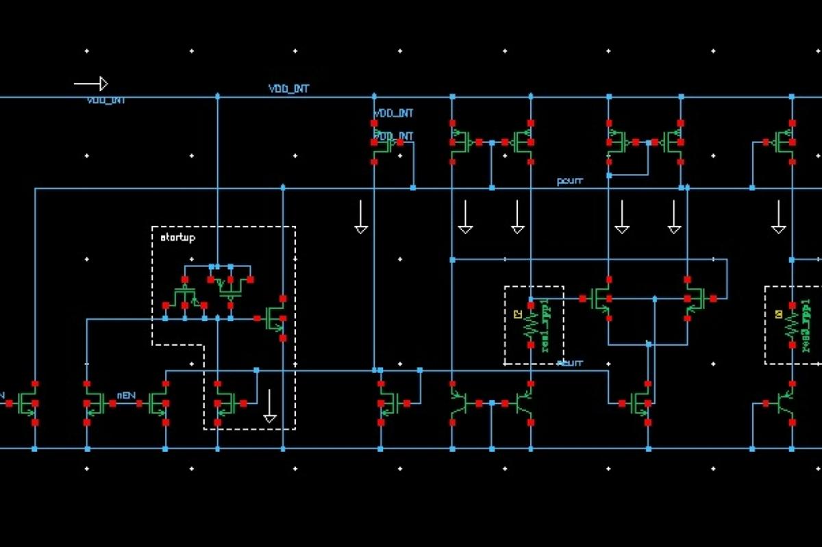
From AI Silicon Observability to Governed Evidence
AI silicon performance now hinges on internal data movement managed by network‑on‑chip (NoC) architectures, but NoC activity alone cannot establish root‑cause of system symptoms. SEGA‑AI introduces a governance layer that qualifies observability data into admissible evidence before any corrective decision...

Which Market Will Dominate the Semiconductor Industry in the Next Decade?
The global semiconductor market, worth $630.5 billion in 2024, is on track to reach $1 trillion by 2030. The United States, despite the CHIPS and Science Act’s $52 billion in manufacturing and R&D incentives, lags in fab capacity and faces a talent shortfall,...

From Billions Of Violations To Actionable Insights: Calibre Vision AI
Calibre Vision AI, launched by Siemens in 2025 and upgraded in 2026, provides AI‑guided, instance‑complete triage of full‑chip DRC results at advanced nodes. The platform now supports real‑time incremental loading of OASIS data, persistent workflow states, and tighter integration with...
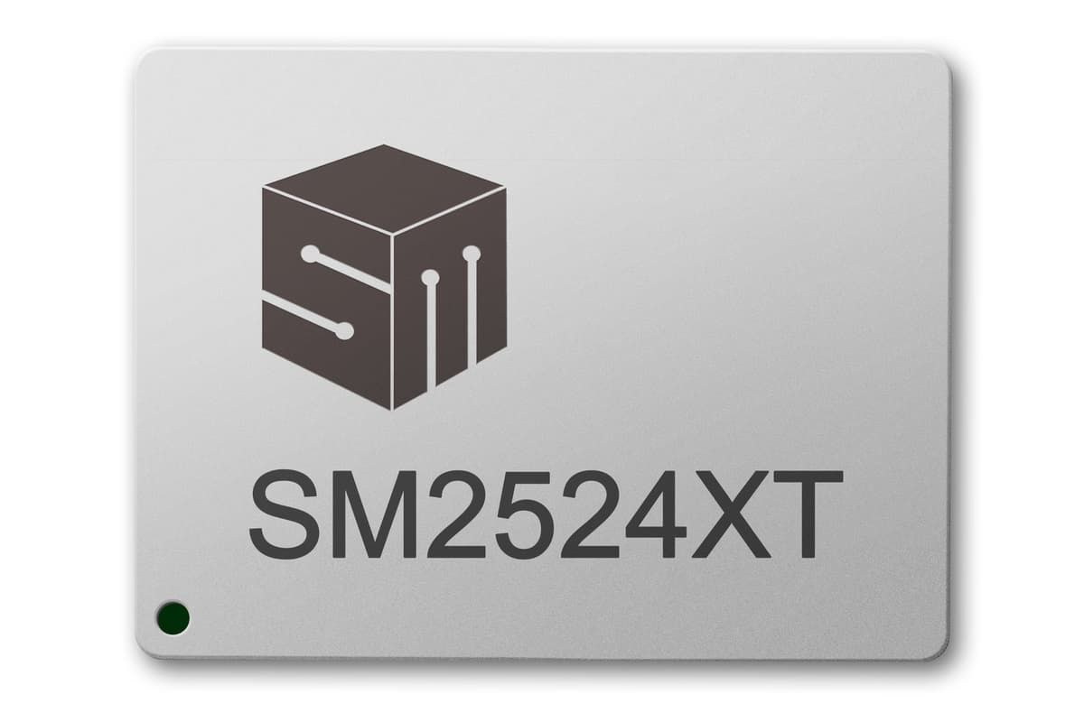
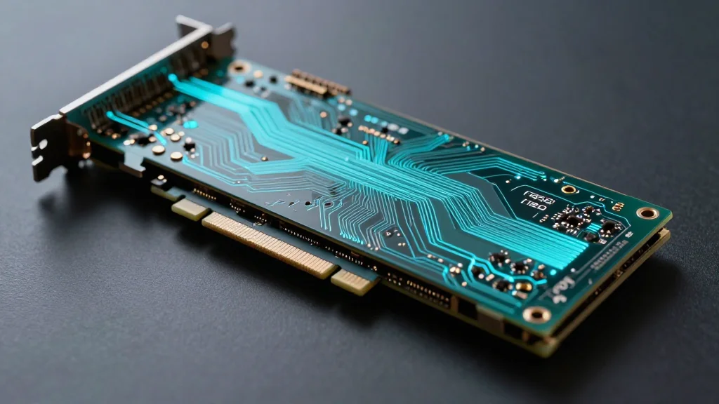
Silicon Motion’s SM2524XT Is a New PCIe Gen5 DRAM-Less SSD Controller for AI PCs
Silicon Motion unveiled the SM2524XT, a PCIe Gen5 DRAM‑less SSD controller aimed at AI‑focused PCs and edge devices. Built on TSMC’s 6 nm process with a quad‑core ARM Cortex‑R8, it promises up to 14 GB/s sequential reads, 12 GB/s writes, and 2.5 million random IOPS...

Nikon to Take on ASML with Low-Priced Chipmaking Equipment: CEO
Nikon announced a strategic push to re‑enter the semiconductor photolithography market by offering equipment at prices lower than those of ASML, which currently controls over 80% of the segment. The move is driven by new President and CEO Yasuhiro Ohmura’s...

Aetina Launches Compact Mini Series Edge AI Systems for Industrial Vision AI and Generative AI Deployment
Aetina announced its Mini Series edge AI systems, built on NVIDIA Jetson Orin Nano and Orin NX modules, delivering up to 157 TOPS in fan‑less, sub‑100 mm enclosures. The four models support dual PoE or MIPI cameras, operate from 12‑24 V DC, and survive...
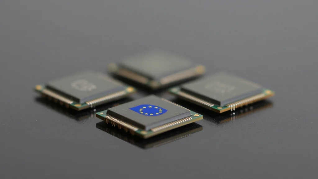
Brussels Eyes Slice of AI Chip Boom
The European Commission is reviving its ambition to produce advanced AI chips in Europe, partnering with Belgium’s Imec and Germany’s SPRIND on a prospective “EU‑made Advanced Semiconductor Manufacturing” plant. The effort is tied to the upcoming Chips Act 2.0, which...
Google Launches a Tiny Board that Runs Gemma 3 Locally
Google unveiled the Coral Board at I/O, a compact single‑board computer that brings on‑device AI to tiny form factors. Powered by a Synaptics Astra SL2619 processor, 2 GB RAM and a 1 TOPS Coral NPU, it can run the open‑source Gemma 3 270M language...
Finding Success in Industry as a Chip Designer
The ASIC market is set to expand from $23.4 billion today to $38.8 billion by 2033, driven by automotive, AI and other specialized applications. Roughly 80% of a modern chip’s die is occupied by pre‑designed silicon IP from firms such as Arm,...
Chipmakers Are Minting Trillion-Dollar Valuations Faster than Ever Before
Three memory‑chip leaders—SK Hynix, Samsung Electronics and Micron Technology—joined the trillion‑dollar club within a 24‑hour window, propelled by soaring AI‑driven demand for high‑bandwidth memory (HBM). Over the past year their shares surged 859% to 1,007%, dwarfing Nvidia’s 58% gain, while...
Taiwan Seeks Reassurances as U.S. Weighs Potential Semiconductor Tariffs
Taiwan’s vice premier Cheng Li‑chiun urged Washington to confirm tariff‑exemption quotas for Taiwanese semiconductors amid U.S. contemplation of Section 232 duties. The January MOU grants Taiwan‑based chip makers export allowances up to 2.5 times their U.S. capacity, and 1.5 times for completed projects,...
ByteDance Is Building Its Own CPUs on Arm and RISC-V to Feed Its AI Infrastructure
ByteDance is developing custom data‑centre CPUs on both Arm and the open‑source RISC‑V architectures to power its rapidly expanding AI infrastructure. The move follows a 25% increase in its AI‑budget to roughly $29.4 bn, as Intel and AMD have raised server‑CPU...
Chiplets, Ecosystems, and Europe’s Post-Fab Semiconductor Strategy
Europe’s semiconductor share is projected to fall to about 6% in 2026, prompting policymakers to pivot from pure fab investment to a broader ecosystem strategy under Chips Act 2.0. The continent is betting on chiplets—modular building blocks linked by advanced packaging—to...

Swapping Out Chiplets: I/Os Vs. Compute
Chiplet‑based architectures let designers replace compute, memory, or I/O dies independently, preserving stable blocks while adopting newer process nodes or faster protocols. Companies often keep I/O dies on mature nodes and upgrade compute chips from 5 nm to 3 nm for power...

Wafer-Scale Vs. Chiplets: The New War? Part 1
Cerebras’ recent IPO highlights a shift in semiconductor strategy as the company scales an entire wafer into a single compute engine, the Wafer‑Scale Engine (WSE‑3). By treating the wafer as one chip, Cerebras has pioneered solutions for yield mapping, distributed...

AMD Expands Versal Prime Gen 2 Lineup With Compact Embedded SoCs
AMD announced three new Versal Prime Gen 2 adaptive SoCs—2VM3454, 2VM3254, and 2VM3104—targeting industrial IoT, robotics, broadcast, Pro AV and edge‑computing. The devices trade eight‑core designs for a compact subsystem with four Cortex‑A78AE cores, six Cortex‑R52 cores and a scaled‑down Mali‑G78AE GPU,...
SK Hynix Thermal Solution Helps Boost AI Performance
SK Hynix unveiled a next‑generation thermal solution that leverages graphene‑based heat spreaders to improve heat dissipation in high‑bandwidth memory (HBM) modules used for AI accelerators. Independent testing showed up to a 12% performance uplift in inference workloads and a 15 °C...
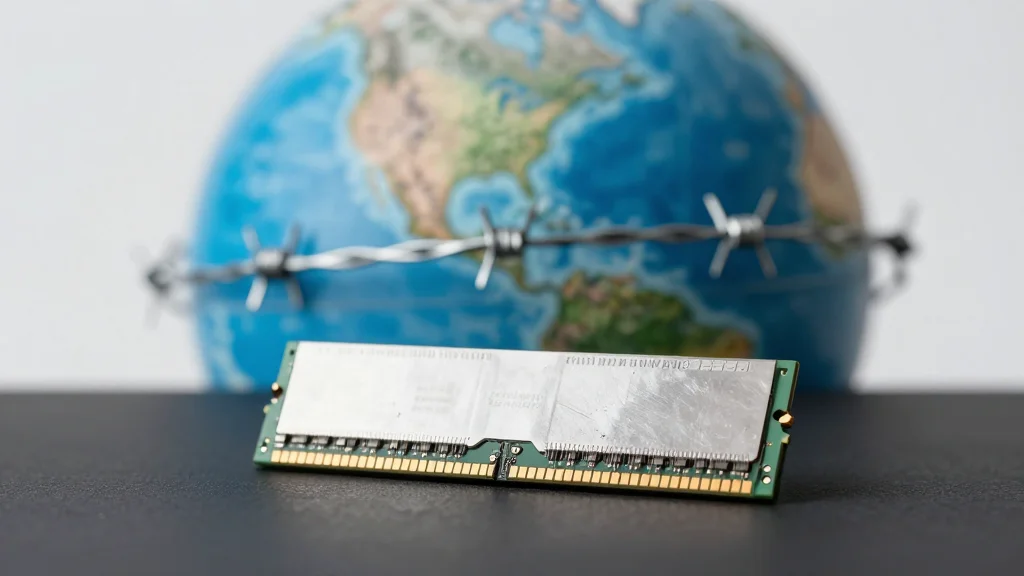
Memory Sourcing Enters a New Era of Geopolitical Fragmentation
Geopolitical tensions between the United States and China are fragmenting the global memory supply chain, forcing advanced DRAM and HBM production into regionally aligned ecosystems while mature memory continues to circulate more broadly. Export controls now shape not only sales...

Marvell, Synopsys Close Lower Despite Forecast-Topping Earnings Buoyed by AI
Marvell Technology and Synopsys reported first‑quarter results that topped analyst expectations, driven by strong AI‑related demand. Marvell posted $2.41 billion in revenue, up 28% YoY, and lifted its full‑year sales outlook to $11.5 billion, while Synopsys posted $2.27 billion in revenue, a 42%...

Marvell’s Stock Falls Despite ‘Exceptional’ AI Demand Driving a Stronger Growth Outlook
Marvell Technology reported fiscal Q1 revenue of $2.418 billion, up 28% year‑over‑year, and raised its full‑year outlook to $11.5 billion—a 40% increase—driven by a 50% surge in its data‑center segment. The company highlighted "exceptional" AI‑related bookings and expects its 800G and 1.6T...