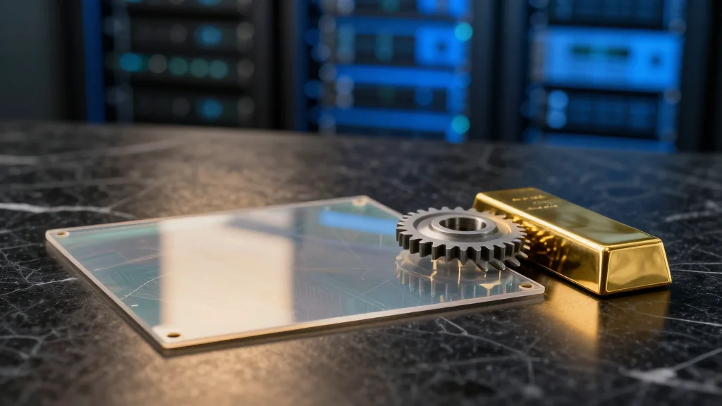
Cyient Semiconductors’ Power Play: How Kinetic Technologies Fits the Puzzle
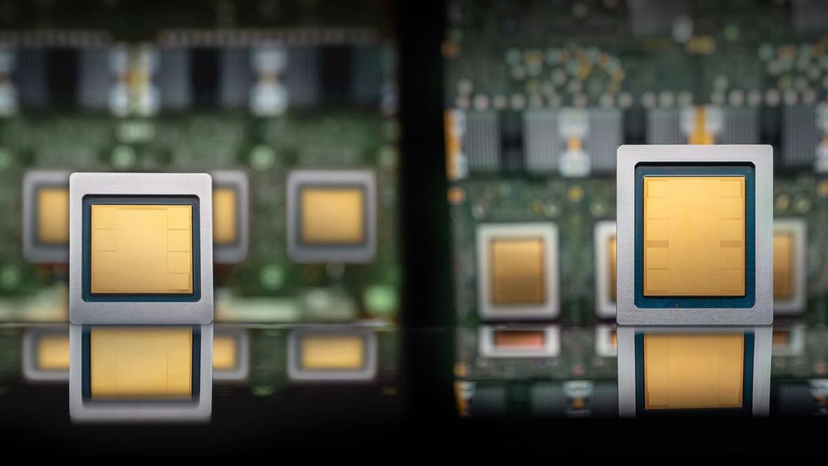
Cyient Semiconductors, India’s largest custom silicon provider, has bought a majority stake in California‑based Kinetic Technologies for $85 million, down from the $93 million initially announced. The deal adds over 100 patents and 250 power‑management ASSPs, potentially doubling Cyient’s addressable market to $8.5 billion. By integrating Kinetic’s low‑voltage protection IP, Cyient aims to build a full‑stack intelligent power platform for data‑center and OEM applications. The company expects the acquisition to become earnings‑per‑share accretive by the second year.
![[Y-Insight] Semiconductor Reliability Emerges as Decisive Factor in New Space Era](/cdn-cgi/image/width=1200,quality=75,format=auto,fit=cover/http://www.thelec.net/news/thumbnail/202604/6747_7080_66_v150.jpg)
[Y-Insight] Semiconductor Reliability Emerges as Decisive Factor in New Space Era
Semiconductor reliability is becoming a decisive factor as the space sector moves into a privately driven New Space era, where launch costs have fallen and commercial off‑the‑shelf (COTS) components are increasingly used. Lee Kwan‑hoon of Korea’s KETI warns that space...

Seeing Clearly Even in the Fog
Korean researchers led by Jong‑Soo Lee have created a next‑generation short‑wave infrared (SWIR) image sensor that fuses Ag₂Te quantum dots with an MoS₂ 2D semiconductor. The hybrid architecture leverages photodoping at the material interface to deliver a responsivity of 7.5 × 10⁵ A/W...

Infineon Joins European Quantum Pilot Lines for Quantum Chips
Infineon announced its participation in three of Europe’s six quantum pilot line projects—CHAMP-ION, SUPREME and SPINS—bringing semiconductor manufacturing expertise to the emerging quantum‑chip ecosystem. The pilot lines are designed to bridge the gap between laboratory prototypes and industrial‑scale production, offering...
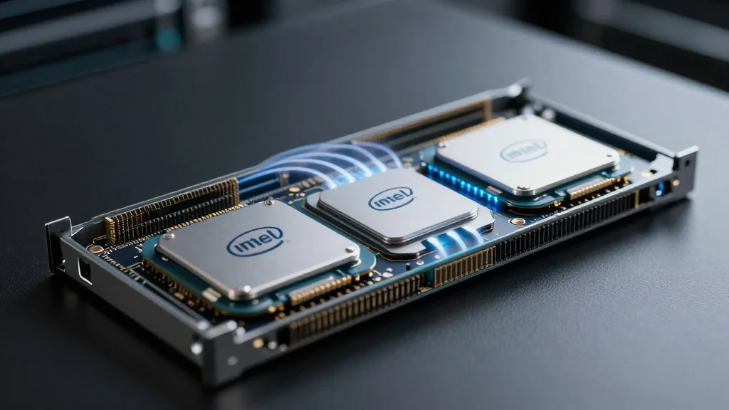
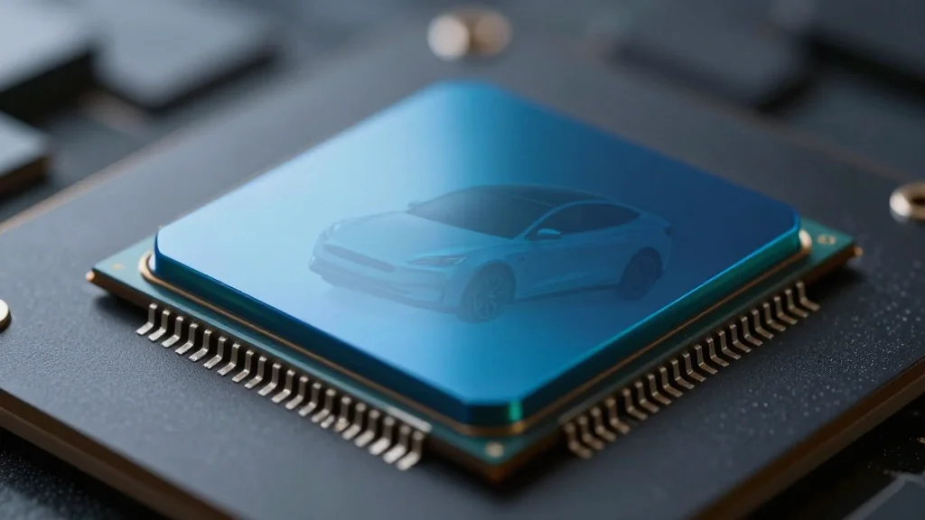
Intel Lands Tesla as First Major Customer for 14A Chip Technology
Tesla announced it will use Intel’s upcoming 14A manufacturing process for chips produced at its planned Terafab AI‑chip complex in Austin. The deal marks Intel’s first major external customer for the 14A node, a critical step as the company seeks...

New Chip Can Protect Wireless Biomedical Devices From Quantum Attacks
MIT engineers have unveiled a needle‑tip ASIC that brings post‑quantum cryptography to wireless biomedical implants such as pacemakers and insulin pumps. The chip achieves 20‑60× higher energy efficiency than existing PQC implementations while adding on‑chip random number generation, side‑channel protection...
YieldWerx Expands Taiwan Presence Through Enlight Technology Collaboration
YieldWerx announced a partnership with Taiwan’s Enlight Technology to bring its data‑driven yield analytics directly into the island’s semiconductor ecosystem. The collaboration will integrate design‑to‑test data across advanced packaging, silicon photonics, and heterogeneous integration, leveraging Enlight’s EDA and MES footprint...
Intel-Google Alliance Signals CPU Resurgence in AI Infrastructure Era
Intel has teamed with Google to pair Xeon CPUs with custom infrastructure processing units (IPUs) for AI workloads, emphasizing a balanced, heterogeneous architecture. The collaboration targets latency‑sensitive inference, data pre‑processing, and system management, offloading networking, storage, and security to IPUs....
Intel Corp (INTC) Q1 2026 Earnings Call Transcript
Intel reported Q1 2026 revenue of $13.3 billion, a 4% sequential increase, but posted a non‑GAAP loss of $0.46 per share after a $3 billion impairment hit gross margin. The company accelerated cost‑cutting, trimming more than 15% of its workforce and slashing...

SiEngine Technology's Qingdao Subsidiary Completes Construction and Begins Operations, Deepening National Industrial Layout
SiEngine Technology's wholly‑owned Qingdao subsidiary has finished construction and started operations, expanding the company's industrial footprint across China. Backed by Ronghui Group, ABC Capital’s Shandong AIC fund and an increased stake from Jingming Capital, the plant includes an R&D center...

Seeds | EVAS Intelligence Secures 1.5 Billion Yuan Series B Funding
EVAS Intelligence secured a Series B financing of 1.5 billion yuan (about $210 million) led by several Beijing development funds and backed by existing investors. The money will fund mass production of the Epoch RISC‑V AI chips, development of the next flagship processor,...
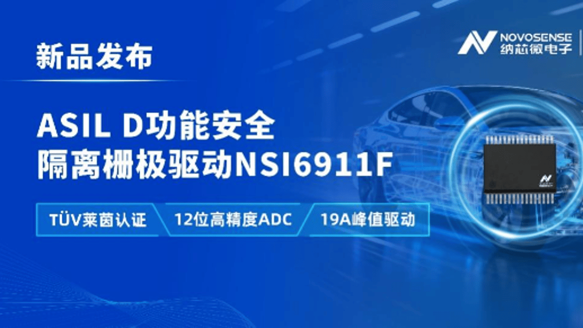
This Domestic Chip Aims to Be the "Safety Cornerstone" Of the 800V Era
Novosense Microelectronics unveiled the NSI6911F series of isolated gate driver chips on April 21, marking the first fully domestic Chinese product that meets ISO 26262 ASIL D safety certification. Designed for 800 V high‑voltage platforms in new‑energy vehicles, the chip delivers 19 A peak...

China Bought Zero H200 Chips ‘as of Today’, Says Lutnick as He Cites ‘Delicate Balance’ with Xi
U.S. Commerce Secretary Howard Lutnick told the Senate that, despite prior approvals, China has bought zero Nvidia H200 AI chips to date. He framed the situation as a "delicate balance" between President Trump’s personal rapport with Xi Jinping and national...
Former Samsung Engineer Gets 7 Years in Prison After Selling Core DRAM Secrets to China’s CXMT for $2 Million
A former Samsung memory engineer received a seven‑year prison term after pleading guilty to selling Samsung's next‑generation DDR5 DRAM design secrets to China’s CXMT for roughly $2 million. The U.S. Department of Justice highlighted the transfer of proprietary schematics and process...
Wolfspeed Appoints Tokyo-Based Regional President for Asia Pacific
Wolfspeed Inc., a leading silicon‑carbide semiconductor maker, announced the appointment of Yasuhisa Harita as regional president for Asia Pacific, effective June 1. Based in Tokyo, Harita will steer commercial strategy across Japan, Korea and the ASEAN nations, targeting revenue growth...

Google’s New TPUs and Agent Platform Offer Expanded AI Solutions
At Google Cloud Next, Google unveiled a new generation of Tensor Processing Units (TPUs) split between training‑focused and inference‑optimized chips, promising lower latency and better performance per watt. It also launched the Gemini Enterprise Agent Platform, which adds orchestration, security...
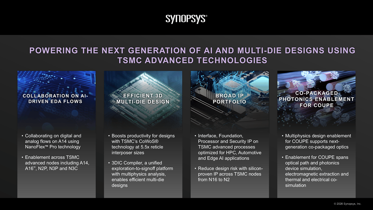
Synopsys Partners with TSMC to Power Next-Generation AI Systems with Silicon Proven IP and Certified EDA Flows
Synopsys announced an expanded partnership with TSMC that integrates AI‑driven EDA flows, silicon‑proven IP, and 3DFabric enablement across the company’s 3 nm, 2 nm and A14/A16 process families. The collaboration delivered the first low‑power M‑PHY v6.0 silicon on TSMC N2P, a 64‑G UCIe...
TSMC Unfolds Map for Process, Packaging Tech
TSMC unveiled its next‑generation roadmap, announcing the 1.4‑nm A14 GAA process for AI data‑center chips in 2028, with A13 and A12 derivatives slated for 2029 that shrink die size by roughly 6%. The company also introduced N2U, a 2‑nm derivative...
Google Unveils Two New AI Chips For the 'Agentic Era'
Google unveiled two new Tensor Processing Units—one dedicated to training and another to inference—targeting what it calls the "agentic era" of AI. The training TPU promises 2.8 times the performance of the seventh‑generation Ironwood chip at the same price, while the...
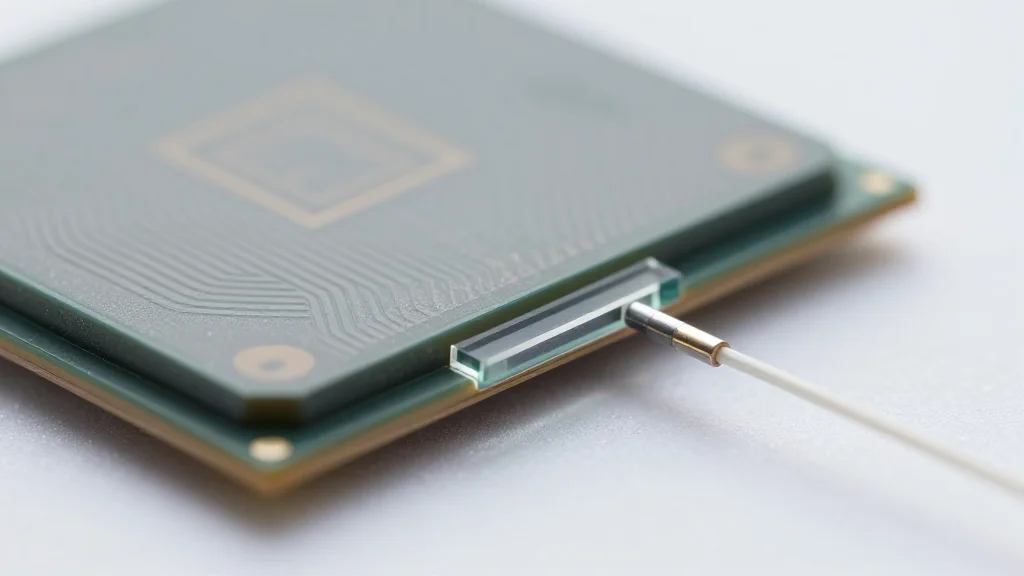
NIST Researchers Develop Photonic Chip Packaging
Researchers at NIST have introduced a new packaging method for photonic integrated circuits that uses hydroxide catalysis bonding, an inorganic glass‑like technique originally developed by NASA. The HCB process creates a molecular‑level bond between optical fibers and chips, allowing the...
Silicon Photonics Just Gained a Powerful New Ally, and It Could Reshape Next-Generation Data Links
Silicon photonics gains a new integration method as imec demonstrates micro‑transfer printing of thin‑film lithium niobate (LiNbO₃) and lithium tantalate (LiTaO₃) onto a CMOS‑compatible platform. The team achieved a 320 Gb/s unamplified O‑band link over 2 km using a 100 GHz germanium photodiode...

Microchip and Sunny Smartlead Expand ASA-ML Ecosystem with ADAS Camera Collaboration
Microchip Technology and Sunny Smartlead have partnered to broaden the Automotive SerDes Alliance Motion Link (ASA‑ML) ecosystem. Sunny Smartlead will launch ADAS camera modules that integrate Microchip’s VS700 ASA‑ML serializers, promising faster, simpler, and lower‑cost development for automotive OEMs and...

The AI Economy Runs on Helium. The Iran War Just Created a $650 Billion Problem
Moody’s Ratings warns that the Iran‑Israel conflict has disrupted Qatar’s Ras Laffan helium plant, creating a $650 billion supply‑chain risk for the AI economy. Helium, essential for wafer cooling, carrier gas and leak detection in semiconductor fabs, has no industrial substitute. The...
AI Chip Startup Blaize and Hardware Developer NeoTensr to Develop Edge Infrastructure for APAC
Blaize and Chinese edge‑hardware firm NeoTensr have signed a contract worth up to $50 million to build AI‑powered edge infrastructure across the APAC region. NeoTensr will integrate Blaize’s Graph Streaming Processor, which can handle more than 200 camera streams per server,...

Market Dynamics and Non-Terrestrial Network (NTN) Chipsets
The global LEO satellite 5G Non‑Terrestrial Network (NTN) chipset market is projected to expand from $6.69 billion in 2026 to $23.07 billion by 2030, a compound annual growth rate above 36 %. This acceleration follows the finalization of 3GPP Release 17 and 18 standards...
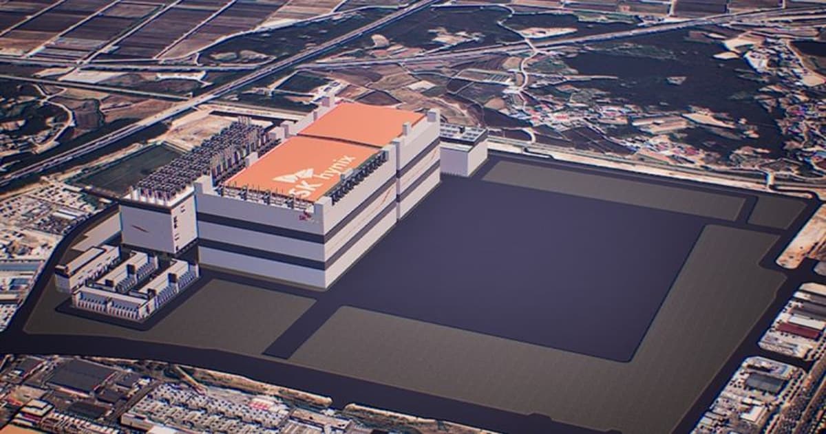
SK Hynix to Invest $12.85bn in Advanced Packaging Plant in Cheongju, South Korea
SK Hynix announced a $12.85 billion investment to build the P&T7 advanced packaging plant in Cheongju, South Korea, with construction starting this month. The 230,000 sqm facility will house three floors of wafer‑level packaging and seven floors of wafer test lines, targeting...
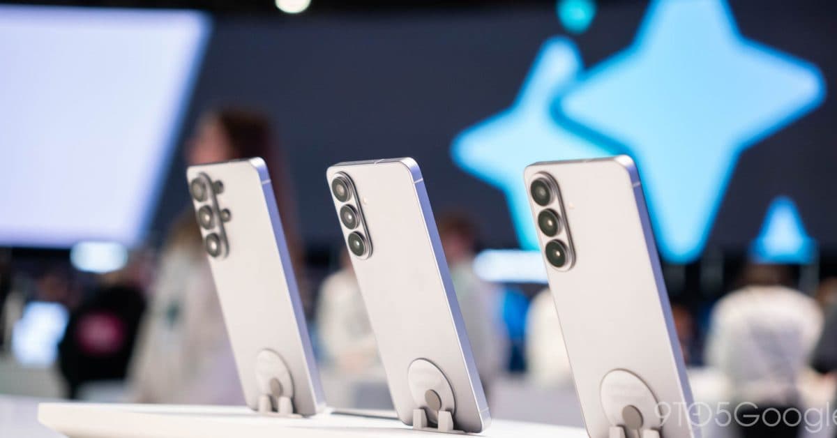
Samsung Is Increasingly Worried About First-Ever Mobile Division Loss in RAM Crisis, Report
Samsung’s mobile division is confronting its first potential operating loss as a global RAM shortage, driven by soaring AI demand, inflates component costs. The company’s head of MX, TM Roh, warned of a possible annual deficit, marking a stark departure...
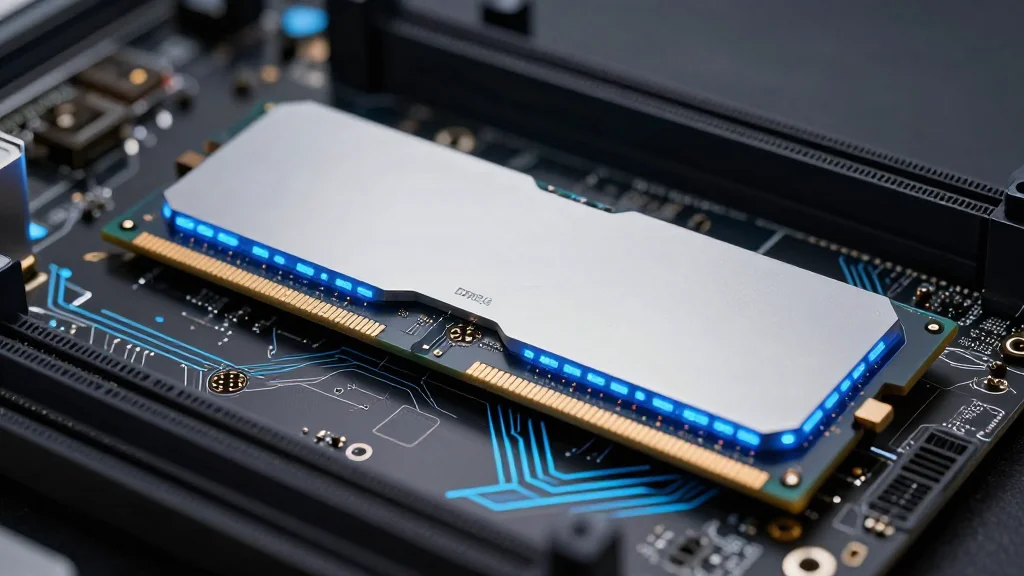
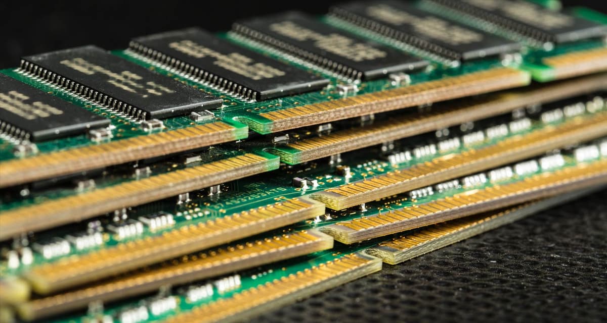
MSI Pushes 128GB DDR5 to 9400 MT/S on X870E Platform
MSI demonstrated a 9400 MT/s DDR5 overclock on its MEG X870E Unify‑X MAX motherboard using a 128 GB configuration of two 64 GB dual‑sided modules. The record was achieved with a new BIOS that MSI plans to release soon, indicating the platform still...

Your Desk Is Now an AI Lab: RP Tech, an NVIDIA Partner, Demos NVIDIA DGX Spark in Bangalore
On April 11, 2026, RP Tech, an NVIDIA partner, showcased the NVIDIA DGX Spark at a Bangalore event, demonstrating a 1.2 kg tabletop AI supercomputer with 128 GB unified memory. The device loaded a 120‑billion‑parameter Nemotron 3 model in quantized form, delivering near‑full GPU utilization for...

Earth Week 2026: Advancing Sustainable Manufacturing for the Essential Technologies the World Relies On
GlobalFoundries (GF) used Earth Week 2026 to detail its 2025 sustainability progress across greenhouse‑gas cuts, energy efficiency, water stewardship, and waste reduction. The company lifted its 2030 Scope 1‑2 emissions target to a 42% absolute reduction, delivering about 105,000 tCO₂e cut in...
Google Cloud Announces Eighth-Generation TPUs, Boasting AI Training and Inference Leaps
Google Cloud unveiled its eighth‑generation tensor processing units, the TPU 8t for training and TPU 8i for inference. The 8t chip is 2.8× faster than the prior Ironwood generation, delivering 121 FP4 exaflops and supporting pods of up to 9,600 chips. The 8i...

We're Launching Two Specialized TPUs for the Agentic Era.
Google announced two new Tensor Processing Units—TPU 8i and TPU 8t—built for the emerging “agentic” AI era. TPU 8i focuses on ultra‑low‑latency inference, enabling autonomous AI agents to reason and act quickly. TPU 8t is optimized for training, offering a massive shared memory pool...
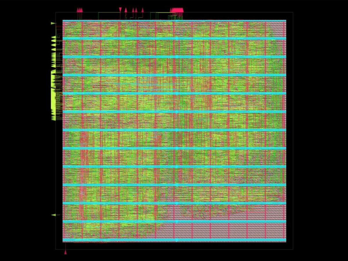
AI Agent Designs a RISC-V CPU Core From Scratch
Verkor.io unveiled VerCore, a RISC‑V CPU core fully designed by its autonomous AI system, Design Conductor. The agent took 12 hours to generate a 1.48 GHz core that scores 3,261 on CoreMark, comparable to Intel’s 2011 Celeron SU2300. Design Conductor orchestrates...

Hong Kong Advances Semiconductor Pilot Lines and Innovation Fund to Strengthen Greater Bay Area Collaboration
Hong Kong’s government announced a suite of measures to deepen Greater Bay Area (GBA) collaboration, centering on semiconductor pilot lines, a new manufacturing innovation centre, and a massive Innovation and Technology Industry‑Oriented Fund (ITIF). The Microelectronics Research and Development Institute...

CVD Equipment Advances SiC Cystal Growth with University Collaboration
CVD Equipment Corporation successfully grew a high‑quality single‑crystal 4H silicon carbide (SiC) boule using its Physical Vapor Transport (PVT) system, in partnership with Stony Brook University. The crystal was shown to be polytype‑free and to have a low defect density,...

AMD Taps GlobalFoundries for MI500 Photonics as It Advances CPO Design
AMD is developing a co‑packaged optics (CPO) version of its Instinct MI500 accelerator, using photonic integrated circuits fabricated by GlobalFoundries and multi‑chip‑module packaging from ASE. The CPO approach aims to boost bandwidth and cut power consumption by placing optical links directly...
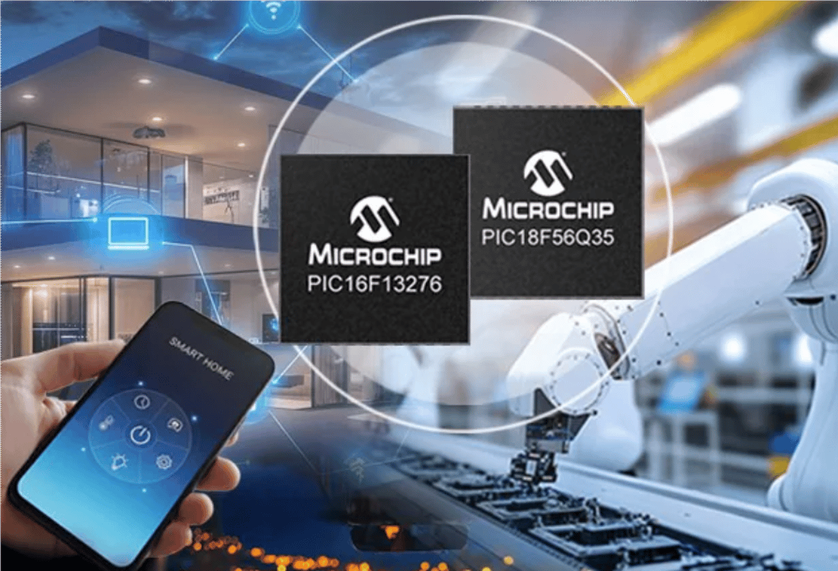
Microchip Launches CLB MCUs to Improve Timing Control and Cut System Cost
Microchip Technology unveiled two new 8‑bit microcontroller families, the PIC16F13276 and PIC18‑Q35, that embed a configurable logic block (CLB) alongside traditional MCU functions. The CLB lets designers shift critical logic from software to hardware, cutting latency and improving predictability for...
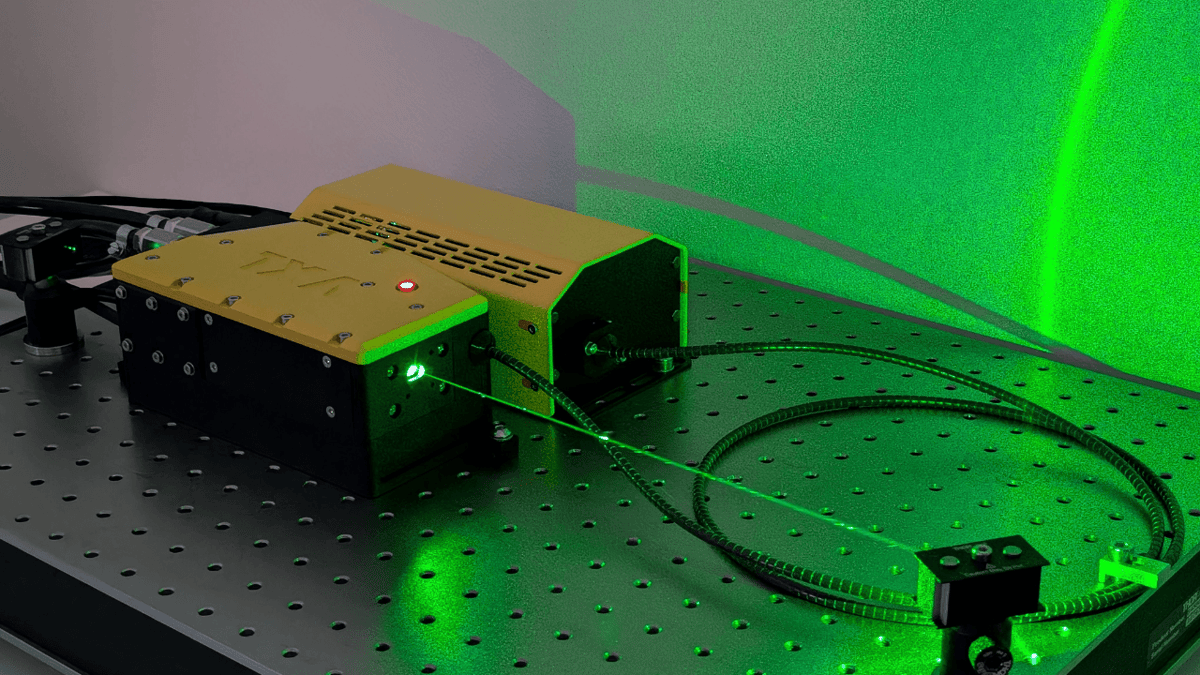
The Quantum Bottleneck Isn’t Chips — It’s Lasers, and Vexlum Wants to Fix It
Vexlum, a Finnish spin‑out focused on III‑V semiconductor lasers, is transitioning from boutique production to its own semiconductor fab to satisfy rising demand for high‑power, low‑noise laser sources. Its VECSEL technology provides compact, multi‑wavelength lasers crucial for quantum computers, atomic...

EU to Launch Chips Act 2.0 in May to Speed Funding and Boost Local Ecosystem
The European Union will unveil Chips Act 2.0 on May 27, tightening the timeline for semiconductor funding and shifting subsidies toward home‑grown firms. The revised framework promises a more direct, faster disbursement process to avoid the delays that have hampered projects under...
High-Throughput Diffuse Electron Projection Lithography
Researchers introduced diffuse electron projection lithography (DEPL), which uses a wide diffuse electron beam in air and patterned gold‑nanoparticle masks to pattern features as small as 4 nm. The technique demonstrated a throughput of 15 4‑inch wafers per hour and projects up...
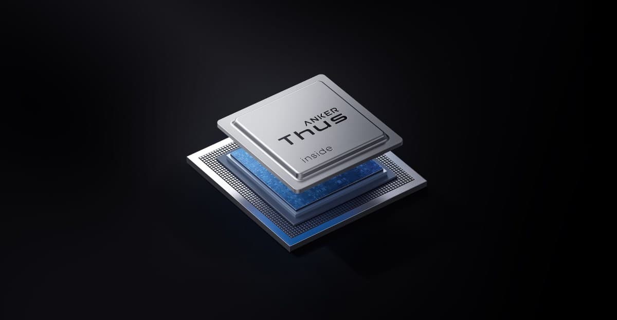
Anker Made Its Own Chip to Bring AI to All Its Products
Anker unveiled the Thus processor, a custom AI chip that uses compute‑in‑memory architecture to embed neural‑net inference directly in audio, mobile accessories, and IoT devices. The chip, smaller and lower‑power than conventional AI silicon, will first appear in Soundcore’s upcoming...
Bosch Sampling Third-Generation SiC Chips to Global Automakers
Bosch has begun sampling its third‑generation silicon carbide (SiC) power chips to automakers worldwide. The new chips deliver about 20% higher performance while being significantly smaller, enabling more chips per wafer and lower costs. Bosch has invested roughly $3.3 billion in...

TU Delft’s Karen Dowling Receives NWO Open Competition ENW-XS Grant
Dr Karen Dowling of TU Delft’s Microelectronics Department secured an NWO Open Competition ENW‑XS grant to study gallium nitride (GaN) for thermoelectric applications in space. Her project will model, fabricate and test 2‑D GaN layers across a temperature span from 500 K...

Chips With Everything: Securing the Silicon Future
U.S. firms must shift from treating semiconductors as a routine procurement category to viewing them as strategic inputs, akin to energy generation capacity. Companies should stratify sourcing by criticality—optimizing commodity parts, securing dual‑source contracts for strategic chips, and building architectural...
Morgan Stanley: Agentic AI Shifts Value From GPUs to CPUs and Memory, Creating up to $60bn Incremental CPU TAM by...
Morgan Stanley’s latest research warns that the next wave of AI – termed “agentic” AI – will shift economic value from GPUs to the broader server stack, especially CPUs and memory. Multi‑step autonomous agents require extensive orchestration, making CPUs the...
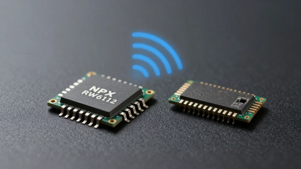
How to Implement OTA Firmware Update on MCUs
The article walks design engineers through implementing over‑the‑air (OTA) firmware updates on NXP’s RW612 MCU using a “staging + copy” workflow. Because the RW612 stores its application image in external serial NOR flash, the update routine relies on NXP’s ROM‑resident FlexSPI API...

Blog Review: Apr. 22
The April 22 blog roundup highlights a series of industry podcasts and posts that dissect critical bottlenecks in chip verification, the rising complexity of analog‑mixed‑signal design, and security threats such as ATM jackpotting. It also showcases new verification IP for...

TSV Complexity Leads To Manufacturing Bottleneck
Through‑silicon vias (TSVs) are essential for 3D stacking and high‑bandwidth memory, but shrinking dimensions are driving up fabrication cost and defect rates. The surge in AI demand has strained HBM and advanced‑assembly capacity, creating a bottleneck in the limited pool...
TSMC Q1 Earnings Call: What It Means for SMH>
Taiwan Semiconductor Manufacturing Company posted a record Q1 2026 revenue of $35.9 billion, a 40.6% year‑over‑year jump, while gross margin rose to 66.2% and net income surged 58.3%. Advanced 3‑nm and 5‑nm nodes generated 61% of the quarter’s sales, underscoring deep...
RAM Price Relief? SK Hynix Plans $13-Billion Korean Fab
SK Hynix announced a $12.85 billion investment to build a new advanced‑packaging fab in South Korea, with construction starting this month. The plant will focus on high‑bandwidth memory (HBM) chips that power AI accelerators, addressing a surge in demand driven by...